The logic gates are the building blocks of digital circuits. A logic gate has one output, but one or more inputs. The output signal appears only for certain combinations of input signals. There are three basic logic gates:
- OR gate,
- AND gate,
- NOT gate.
Each logic gate is indicated by a logical symbol and its function is described either by a ‘Truth table’ or by a ‘Boolean expression’
Truth Table of Logic Gates
A logic gate may have one or more inputs, but only one output. The relation between the possible values of input and output signals are expressed in a table which is called the “truth table”.
Thus, the truth table of a logic gate is a table that shows all possible input combinations and the corresponding outputs for the logic gate.
Boolean Expression of Logic Gates
George Boole invented a different kind of algebra based on logical statements that have only two values, namely either a ‘true’ value or a ‘false’ value. The logical statements are called ‘Boolean variables’
The true value of a Boolean variable is denoted by the binary number 1 and the false value by the binary number 0.
The expression showing the combination of two Boolean variables that result in a new Boolean variable is known as the Boolean expression.
The OR Logic Gate
The OR gate is a device that has two (or more) input variables A and B and one output variable Y. The Boolean expression for the OR gate is:
A + B = Y
The possible combinations of the input A and B and the output Y of the OR gate can be illustrated with the help of an electrical circuit shown in Figure.
In this circuit, two switches A and B (inputs) are connected in parallel with a battery and a bulb Y (output).
The opening and closing of the switches A and B correspond to binary numbers 0 and 1 respectively. Similarly, if the bulb remains OFF, the output Y is 0; if it glows, the output Y is 1.

- If both switches are open (A = 0, B = 0) the bulb will not glow (Y = 0).
- If switch A is open and B is closed (A = 0, B =1) the bulb will glow (Y = 1).
- If switch A is closed and B is open (A = 1, B =0) the bulb will glow (Y = 1).
- If both switches are closed (A = 1, B = 1) the bulb will glow (Y= 1).
These possible combinations of A, B and Y are shown in Figure in the form of a table which is the truth table of OR logic gate.
Therefore, the working of the OR gate can be stated as: the output Y will be 1 when the input A or B or both are 1.
The AND Logic Gate
The AND gate is also a two-input and one-output logic gate. Its Boolean expression is as follows:
A*B = Y
The possible combinations of the inputs A and B and the output Y of the AND logic gate can be illustrated with the help of the electric circuit shown in Figure.
In this circuit, two switches A and B (inputs) are connected in series with a battery and a bulb Y (output). The working of circuit is as follows:

- If both switches are open (A = 0, B = 0) the bulb will not glow (Y = 0).
- If switch A is open and B is closed (A = 0, B = 1) the bulb will not glow (Y = 0).
- If switch A is closed and B is open (A = 1, B =0) the bulb will not glow (Y = 0).
- If both switches are closed (A = 1, B = 1) the bulb will glow (Y = 1).
These possible combinations of A, B and shown in Figure in the form of a table which is the truth table of AND logic gate.
Therefore, the working of the AND gate can be stated as: the output Y will be 1 when both the inputs A and B are 1 otherwise Y will be zero.
The NOT Logic Gate
The not gate has only one input and the one output. It combines the input A with the output Y according to the Boolean expression:
Y = Ā (read as Y equals NOT A)
It means that Y is an inversion of A.
The logic symbol of the NOT gate is shown in Figure. The possible combinations of the input A and the output Y of the NOT gate can be illustrated with the help of the electric circuit shown in Figure. In this circuit, a switch A (input), a battery and a bulb Y (output) is connected as shown in Figure.

- If switch A is open (A = 0), the bulb will glow (Y = 1).
- If switch is closed (A = 1), the current finds an easier path through R. Hence it does not flow through the bulb and so the bulb will not glow (Y = 0).
Combination of Basic Logic Gates
The various combination of the three basic gates, namely, OR, AND and NOT can produce three more important gates. These are NAND gate, NOR gate, and XOR gate.
The NAND Logic Gate
The NAND gate is a combination of AND and NOT gates. If the output of AND gate is connected to the input of NOT gate as shown in Figure, the gate so obtained is called NAND gate.

The NAND gate truth table can be illustrated by a simple circuit consisting of two switches A and B, a battery and a bulb Y connected as shown in Figure. A small resistance R is added to limit the current when both switches are closed.
- When the switches A and B both are open ( A = 0, B = 0), the bulb glows (Y = 1). This illustrates the first row of the truth table.
- When either A alone is open (A = 0, B = 1) or B alone is open (A = 1, B = 0), the bulb glows (Y = 1). This illustrates the second and third row of the truth table.

- If both A and B are closed (A = 1, B = 1) the current finds an easier path through R, A and B and hence the bulb does not glow (Y = 0). This illustrates the fourth row of the table.
The NAND output is an inverse of AND output. This means that an input giving 1 output in AND gate will give zero output in NAND gate and vice-versa.
For example, in AND gate, the output Y is 1 only when both A and B are 1, but in NAND gate, Y will be zero for such a case. Similarly, when both inputs A and B are not simultaneously 1, then output is 0 in AND gate but it is 1 in NAND gate.
The NAND gate is a universal gate because it can perform all logic operations of OR gate, AND gate and NOT gate, as shown ahead.
The NOR Logic Gate
The NOR gate is a combination of OR and NOT gates. If the output of OR gate is connected to the input of NOT gate, as shown in Figure, the resulting gate is called the NOR gate.

The NOR gate truth table can be illustrated by a simple circuit shown in Figure.
- When the switches A and B both are open (A = 0, B = 0), the bulb glows (Y = 1). This illustrates the first row of the truth table.

- When either A alone is closed (A = 1, B = 0) or B alone is closed (A = 0, B = 1) or both A and B are closed (A = 1, B = 1), the current always finds an easier path to flow. Hence it does not flow through the bulb and so the bulb does not glow (Y = 0). This illustrates the second, third and fourth row of the truth table.
Thus the NOR output is inverse of OR output.
NAND | NOR Gate as Building Block in Digital Circuits
None of the basic logic gates (OR, AND and NOT) alone can produce a different gate by repeated use. However, the repeated use of NAND (or NOR) gate can produce all three basic logic gates. Hence the NAND (or NOR) gate serves as a building block in digital circuits.
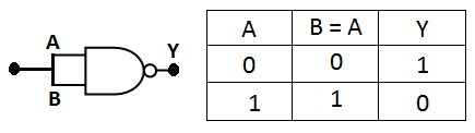
Obtaining NOT Gate from NAND Gate
If the two inputs A and B of the NAND gate are joined together to make one input, as shown in Figure, then the NAND gate works as a NOT gate. This is so because by using B = A in the truth table of NAND gate we obtain the truth table shown in Figure, which is the truth table of NOT gate.
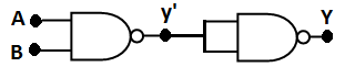
Obtaining AND Gate from NAND Gate
If the output of the NAND gate is connected to the input of NOT gate (made from NAND gate by joining its two inputs together), as shown in Figure then the combination works as an AND gate.
Obtaining OR Gate from NAND Gate
If the inputs A and B are inverted by using two NOT gates (obtained from two NAND gates) and the resulting outputs are fed to a third NAND gate as shown in Figure, then the final output Y is the same as of an OR gate. In other words, the arrangement works as OR gate.

Thanks for reading about ‘logic gates circuit diagram and working’.
your explanations are very clear and understanding aswell as the digrams. l really liked the presentation