TTL Logic Family
TTL stands for transistor transistor logic. It is a logic family implemented with bipolar process technology that combines or integrates NPN transistors, PN junction diodes and diffused resistors in a single monolithic structure to get the desired logic function. The NAND gate is the basic building block of this logic family.
Different subfamilies in this logic family, include standard TTL, low-power TTL, high-power TTL, low-power Schottky TTL, Schottky TTL, advanced low-power Schottky TTL, advanced Schottky TTL and fast TTL. In the following paragraphs, we will briefly describe each of these subfamilies in terms of internal structure and characteristic parameters.
Standard TTL
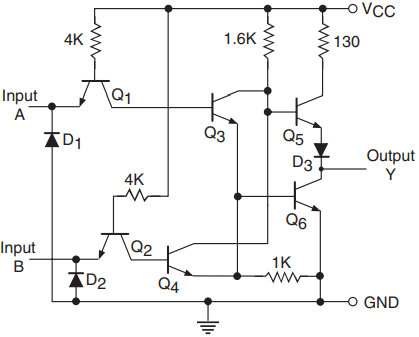
Figure 1 shows the internal schematic of a standard TTL NAND gate. It is one of the four circuits of 5400/7400, which is a quad two-input NAND gate. The circuit operates as follows.
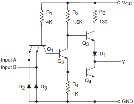
Transistor Q1 is a two-emitter NPN transistor, which is equivalent to two NPN transistors with their base and emitter terminals tied together. The two emitters are the two inputs of the NAND gate. Diodes D2 and D3 are used to limit negative input voltages. We will now examine the behaviour of the circuit for various possible logic states at the two inputs.
Circuit Operation: When both the inputs are in the logic HIGH state as specified by the TTL family (VIH = 2 V minimum), the current flows through the base-collector PN junction diode of transistor Q1 into the base of transistor Q2. Transistor Q2 is turned ON to saturation, with the result that transistor Q3 is switched OFF and transistor Q4 is switched ON.
This produces a logic LOW at the output, with VOL being 0.4 V maximum when it is sinking a current of 16 mA from external loads represented by inputs of logic functions being driven by the output. The current-sinking action is shown in Fig. 2(a).
Transistor Q4 is also referred to as the current-sinking or pull-down transistor, for obvious reasons. Diode D1 is used to prevent transistor Q3 from conducting even a small amount of current when the output is LOW.
When the output is LOW, Q4 is in saturation and Q3 will conduct slightly in the absence of D1. Also, the input current IIH in the HIGH state is nothing but the reverse-biased junction diode leakage current and is typically 40 A.
When either of the two inputs or both inputs are in the logic LOW state, the base-emitter region of Q1 conducts current, driving Q2 to cut-off in the process. When Q2 is in the cut-off state, Q3 is driven to conduction and Q4 to cut-off. This produces a logic HIGH output with VOH(min.) = 2.4 V guaranteed for minimum supply voltage VCC and a source current of 400 A. The current-sourcing action is shown in Fig. 5.7(b).
Transistor Q3 is also referred to as the current-sourcing or pull-up transistor. Also, the LOW-level input current IIL, given by (VCC − VBE1)/R1, is 1.6 mA (max.) for maximum VCC.
Totem-Pole Output Stage: Transistors Q3 and Q4 constitute what is known as a totem-pole output arrangement. In such an arrangement, either Q3 or Q4 conducts at a time depending upon the logic status of the inputs. The totem-pole arrangement at the output has certain distinct advantages. The major advantage of using a totem-pole connection is that it offers low-output impedance in both the HIGH and LOW output states.
In the HIGH state, Q3 acts as an emitter follower and has an output impedance of about 70 . In the LOW state, Q4 is saturated and the output impedance is approximately 10 . Because of the low output impedance, any stray capacitance at the output can be charged or discharged very rapidly through this low impedance, thus allowing quick transitions at the output from one state to the other.
Another advantage is that, when the output is in the logic LOW state, transistor Q4 would need to conduct a fairly large current if its collector were tied to VCC through R3 only. A non-conducting Q3 overcomes this problem.
A disadvantage of the totem-pole output configuration results from the switch-off action of Q4 being slower than the switch-on action of Q3. On account of this, there will be a small fraction of time, of the order of a few nanoseconds, when both the transistors are conducting, thus drawing heavy current from the supply.
Characteristic Features: To sum up, the characteristic parameters and features of the standard TTL family of devices include the following:
- VIL = 0.8 V; VIH = 2 V; IIH = 40 µA; IIL = 1.6 mA; VOH = 2.4 V; VOL = 0.4 V; IOH = 400µ A; IOL = 16 mA;
- VCC = 4.75 – 5.25 V (74-series) and 4.5 – 5.5 V (54-series);
- propagation delay (for a load resistance of 400Ω, a load capacitance of 15 pF and an ambient temperature of 25 °C) = 22 ns (max.) for LOW-to-HIGH transition at the output and 15 ns (max.) for HIGH-to-LOW output transition;
- worst-case noise margin = 0.4 V; fan-out = 10;
- ICCH (for all four gates) = 8 mA; ICCL (for all four gates) = 22 mA;
- operating temperature range = 0–70 °C (74- series) and −55 to +125 °C (54-series);
- speed–power product = 100 pJ;
- maximum flip-flop toggle frequency = 35 MHz.
Other Logic Gates in Standard TTL
As outlined earlier, the NAND gate is the fundamental building block of the TTL family. In the following paragraphs we will look at the internal schematics of the other logic gates and find for ourselves their similarity to the schematic of the NAND gate discussed in detail in earlier paragraphs.
NOT Gate (or Inverter): Figure 3 shows the internal schematic of a NOT gate (inverter) in the standard TTL family. The schematic shown is that of one of the six inverters in a hex inverter (type 7404/5404). The internal schematic is just the same as that of the NAND gate except that the input transistor is a normal single emitter NPN transistor instead of a multi-emitter one. The circuit is self-explanatory.
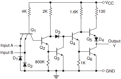
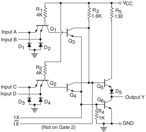
NOR Gate: Figure 4 shows the internal schematic of a NOR gate in the standard TTL family. The schematic shown is that of one of the four NOR gates in a quad two-input NOR gate (type 7402/5402).
On the input side there are two separate transistors instead of the multi-emitter transistor of the NAND gate. The inputs are fed to the emitters of the two transistors, the collectors of which again feed the bases of the two transistors with their collector and emitter terminals tied together. The resistance values used are the same as those used in the case of the NAND gate. The output stage is also the same totem-pole output stage. The circuit is self-explanatory.
The only input condition for which transistors Q3 and Q4 remain in cut-off, thus driving Q6 to cut-off and Q5 to conduction, is the one when both the inputs are in the logic LOW state. The output in such a case is logic HIGH. For all other input conditions, either Q3 or Q4 will conduct, driving Q6 to saturation and Q5 to cut-off, producing a logic LOW at the output.
AND Gate: Figure 5 shows the internal schematic of an AND gate in the standard TTL family. The schematic shown is that of one of the four AND gates in a quad two-input AND gate (type 7408/5408). In order to explain how this schematic arrangement behaves as an AND gate, we will begin by investigating the input condition that would lead to a HIGH output.
A HIGH output implies Q6 to be in cut-off and Q5 to be in conduction. This can happen only when Q4 is in cut-off. Transistor Q4 can be in the cut-off state only when both Q2 and Q3 are in conduction. This is possible only when both inputs are in the logic HIGH state.
Let us now see what happens when either of the two inputs is driven to the LOW state. This drives Q2 and Q3 to the cut-off state, which forces Q4 and subsequently Q6 to saturation and Q5 to cut-off.
OR Gate: Figure 6 shows the internal schematic of an OR gate in the standard TTL family. The schematic shown is that of one of the four OR gates in a quad two-input OR gate (type 7432/5432). We will begin by investigating the input condition that would lead to a LOW output.
A LOW output demands a saturated Q8 and a cut-off Q7. This in turn requires Q6 to be in saturation and Q5, Q4 and Q3 to be in cut-off. This is possible only when both Q1 and Q2 are in saturation. That is, both inputs are in the logic LOW state. This verifies one of the entries of the truth table of the OR gate.
Let us now see what happens when either of the two inputs is driven to the HIGH state. This drives either of the two transistors Q3 and Q4 to saturation, which forces Q5 to saturation and Q6 to cut-off. This drives Q7 to conduction and Q8 to cut-off, producing a logic HIGH output.
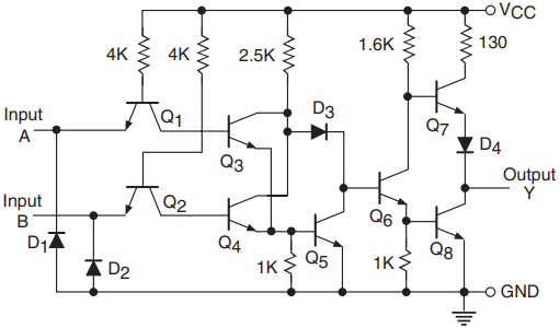
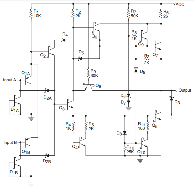
EXCLUSIVE-OR Gate: Figure 7 shows the internal schematic of an EX-OR gate in the standard TTL family. The schematic shown is that of one of the four EX-OR gates in a quad two-input EX-OR gate (type 7486/5486). We will note the similarities between this circuit and that of an OR gate. The only new element is the interconnected pair of transistors Q7 and Q8. We will see that, when both the inputs are either HIGH or LOW, both Q7 and Q8 remain in cut-off.
In the case of inputs being in the logic HIGH state, the base and emitter terminals of both these transistors remain near the ground potential. In the case of inputs being in the LOW state, the base and emitter terminals of both these transistors remain near VCC. The result is conducting Q9 and Q11 and non-conducting Q10, which leads to a LOW output.
When either of the inputs is HIGH, either Q7 or Q8 conducts. Transistor Q7 conducts when input B is HIGH, and transistor Q8 conducts when input A is HIGH. Conducting Q7 or Q8 turns off Q9 and Q11 and turns on Q10, producing a HIGH output. This explains how this circuit behaves as an EX-OR gate.
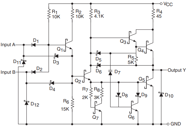
AND-OR-INVERT Gate: Figure 8 shows the internal schematic of a two-wide, two-input AND-OR-INVERT or AND-NOR gate. The schematic shown is that of one of the two gates in a dual two-wide, two-input AND-OR-INVERT gate (type 7450/5450). The two multi-emitter input transistors Q1 and Q2 provide ANDing of their respective inputs. Drive splitters comprising Q3, Q4, R3 and R4 provide the OR function. The output stage provides inversion.
The number of emitters in each of the input transistors determines the number of literals in each of the minterms in the output sum-of-products Boolean expression. How wide the gate is going to be is decided by the number of input transistors, which also equals the number of drive splitter transistors.
Open Collector Gate: An open collector gate in TTL is one that is without a totem-pole output stage. The output stage in this case does not have the active pull-up transistor. An external pull-up resistor needs to be connected from the open collector terminal of the pull-down transistor to the VCC terminal. The pull-up resistor is typically 10 k.
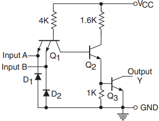
Figure 9 shows the internal schematic of a NAND gate with an open collector output. The schematic shown is that of one of the four gates of a quad two-input NAND (type 74/5401). The advantage of open collector outputs is that the outputs of different gates can be wired together, resulting in ANDing of their outputs.
It may be mentioned here that the outputs of totem-pole TTL devices cannot be tied together. Although a common tied output may end up producing an ANDing of individual outputs, such a connection is impractical. This is illustrated in Fig. 20, where outputs of two totem-pole output TTL gates have been tied together.
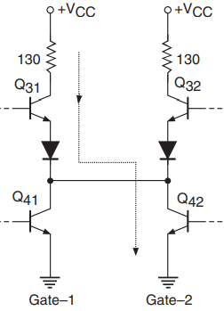
Let us assume that the output of one of the gates, say gate-2, is LOW, and the output of the other is HIGH. The result is that a relatively heavier current flows through Q31 and Q42. This current, which is of the order of 50–60 mA, exceeds the IOL(max.) rating of Q42. This may eventually lead to both transistors getting damaged. Even if they survive, VOL(max.) of Q42 is no longer guaranteed.
In view of this, although totem-pole output TTL gates are not tied together, an accidental shorting of outputs is not ruled out. In such a case, both devices are likely to get damaged. In the case of open collector devices, deliberate or non-deliberate, shorting of outputs produces ANDing of outputs with no risk of either damage or compromised performance specifications.
Tristate Gate: A tristate gate has three output states, namely the logic LOW state, the logic HIGH state and the high-impedance state. An external enable input decides whether the logic gate works according to its truth table or is in the high-impedance state.
Figure 11 shows the typical internal schematic of a tristate inverter with an active HIGH enable input. The circuit functions as follows.
When the enable input is HIGH, it reverse-biases diode D1 and also applies a logic HIGH on one of the emitters of the input transistor Q1. The circuit behaves like an inverter. When the enable input is LOW, diode D1 becomes forward biased. A LOW enable input forces Q2 and Q4 to cut-off. Also, a forward-biased D1 forces Q3 to cut-off. With both output transistors in cut-off, the output essentially is an open circuit and thus presents high output impedance.
Subfamilies of TTL Logic Family
Low Power TTL
The low-power TTL is a low-power variant of the standard TTL where lower power dissipation is achieved at the expense of reduced speed of operation. Figure 12 shows the internal schematic of a low-power TTL NAND gate. The circuit shown is that of one of the four gates inside a quad two-input NAND (type 74L00 or 54L00).
The circuit, as we can see, is the same as that of the standard TTL NAND gate except for an increased resistance value of the different resistors used in the circuit. Increased resistance values lead to lower power dissipation.
Characteristic Features: Characteristic features of this family are summarized as follows:
- VIH = 2 V; VIL = 0.7 V; IIH = 10µ A; IIL = 0.18 mA; VOH = 2.4 V; VOL = 0.4 V; IOH = 200 µA; IOL = 3.6 mA; VCC = 4.75 – 5.25 V (74-series) and 4.5 – 5.5 V (54-series);
- propagation delay (for a load resistance of 400Ω , a load capacitance of 50 pF, VCC = 5 V and an ambient temperature of 25 °C) = 60 ns (max.) for both LOW-to-HIGH and HIGH-to-LOW output transitions;
- worst-case noise margin = 0.3 V; fan-out = 20; ICCH (for all four gates) = 0.8 mA; ICCL (for all four gates) = 2.04 mA;
- operating temperature range = 0 – 70 °C (74- series) and −55 to +125 °C (54-series);
- speed–power product = 33 pJ; maximum flip-flop toggle frequency = 3 MHz.
High Power TTL (74H/54H)
The high-power TTL is a high-power, high-speed variant of the standard TTL where improved speed (reduced propagation delay) is achieved at the expense of higher power dissipation. Figure 13 shows the internal schematic of a high-power TTL NAND gate. The circuit shown is that of one of the four gates inside a quad two-input NAND (type 74H00 or 54H00).
The circuit, as we can see, is nearly the same as that of the standard TTL NAND gate except for the transistor Q3–diode D1 combination in the totem-pole output stage having been replaced by a Darlington arrangement comprising Q3, Q5 and R5.
The Darlington arrangement does the same job as diode D1 in the conventional totem-pole arrangement. It ensures that Q5 does not conduct at all when the output is LOW. The decreased resistance values of different resistors used in the circuit lead to higher power dissipation.
Characteristic Features: Characteristic features of this family are summarized as follows:
- VIH = 2 V; VIL = 0.8 V; IIH = 50 µA; IIL = 2 mA; VOH = 2.4 V; VOL = 0.4 V; IOH = 500 µA; IOL = 20 mA;
- VCC = 4.75 – 5.25 V (74-series) and 4.5 – 5.5 V (54-series);
- propagation delay (for a load resistance of 280Ω a load capacitance of 25 pF, VCC = 5 V and an ambient temperature of 25 °C) = 10 ns (max.) for both LOW-to-HIGH and HIGH-to-LOW output transitions;
- worst–case noise margin = 0.4 V; fan-out = 10; ICCH (for all four gates) = 16.8 mA; ICCL (for all four gates) = 40 mA;
- operating temperature range = 0 – 70 °C (74-series) and −55 to +125 °C (54-series);
- speed–power product = 132 pJ; maximum flip-flop frequency = 50 MHz.
Schottky TTL (74S/54S)
The Schottky TTL offers a speed that is about twice that offered by the high-power TTL for the same power consumption. Figure 14 shows the internal schematic of a Schottky TTL NAND gate. The circuit shown is that of one of the four gates inside a quad two-input NAND (type 74S00 or 54S00).
The circuit, as we can see, is nearly the same as that of the high-power TTL NAND gate. The transistors used in the circuit are all Schottky transistors with the exception of Q5. A Schottky Q5 would serve no purpose, with Q4 being a Schottky transistor.
A Schottky transistor is nothing but a conventional bipolar transistor with a Schottky diode connected between its base and collector terminals. The Schottky diode with its metal–semiconductor junction not only is faster but also offers a lower forward voltage drop of 0.4 V as against 0.7 V for a P–N junction diode for the same value of forward current.
The presence of a Schottky diode does not allow the transistor to go to deep saturation. The moment the collector voltage of the transistor tends to go below about 0.3 V, the Schottky diode becomes forward biased and bypasses part of the base current through it. The collector voltage is thus not allowed to go to the saturation value of 0.1 V and gets clamped around 0.3 V.
While the power consumption of a Schottky TTL gate is almost the same as that of a high-power TTL gate owing to nearly the same values of the resistors used in the circuit, the Schottky TTL offers a higher speed on account of the use of Schottky transistors.
Characteristic Features: Characteristic features of this family are summarized as follows:
- VIH = 2 V; VIL = 0.8 V; IIH = 50 µA; IIL = 2 mA; VOH = 2.7 V; VOL = 0.5 V; IOH = 1 mA; IOL = 20 mA;
- VCC = 4.75 – 5.25 V (74-series) and 4.5 – 5.5 V (54-series);
- propagation delay (for a load resistance of 280Ω , a load capacitance of 15 pF, VCC = 5 V and an ambient temperature of 25 °C) = 5 ns (max.) for LOW-to-HIGH and 4.5 ns (max.) for HIGH-to-LOW output transitions;
- worst-case noise margin = 0.3 V; fan-out = 10; ICCH (for all four gates) = 16 mA; ICCL (for all four gates) = 36 mA;
- operating temperature range = 0 – 70 °C (74- series) and −55 to +125 °C (54-series); speed–power product = 57 pJ;
- maximum flip-flop toggle frequency = 125 MHz.
Low Power Schottky TTL (74LS/54LS)
The low-power Schottky TTL is a low power consumption variant of the Schottky TTL. Figure 15 shows the internal schematic of a low-power Schottky TTL NAND gate. The circuit shown is that of one of the four gates inside a quad two-input NAND (type 74LS00 or 54LS00).
We can notice the significantly increased value of resistors R1 and R2 used to achieve lower power consumption. Lower power consumption, of course, occurs at the expense of reduced speed or increased propagation delay. Resistors R3 and R5, which primarily affect speed, have not been increased in the same proportion with respect to the corresponding values used in the Schottky TTL as resistors R1 and R2.
That is why, although the low-power Schottky TTL draws an average maximum supply current of 3 mA (for all four gates) as against 26 mA for the Schottky TTL, the propagation delay is 15 ns in LS-TTL as against 5 ns for S-TTL. Diodes D3 and D4 reduce the HIGH-to-LOW propagation delay. While D3 speeds up the turn-off of Q4, D4 sinks current from the load.
Another noticeable difference in the internal schematics of the low-power Schottky TTL NAND and Schottky TTL NAND is the replacement of the multi-emitter input transistor of the Schottky TTL by diodes D1 and D2 and resistor R1. The junction diodes basically replace the two emitter-base junctions of the multi-emitter input transistor Q1 of the Schottky TTL NAND (Fig. 14).
The reason for doing so is that Schottky diodes can be made smaller than the transistor and therefore will have lower parasitic capacitances. Also, since Q1 of LS-TTL (Fig. 15) cannot saturate, it is not necessary to remove its base charge with a bipolar junction transistor.
Characteristic Features: Characteristic features of this family are summarized as follows:
- VIH = 2 V; VIL = 0.8 V; IIH = 20µA; IIL = 0.4 mA; VOH = 2.7 V; VOL = 0.5 V; IOH = 0.4 mA; IOL = 8 mA;
- VCC = 4.75 – 5.25 V (74-series) and 4.5 – 5.5 V (54-series);
- propagation delay (for a load resistance of 280Ω , a load capacitance of 15 pF, VCC = 5 V and an ambient temperature of 25 °C) = 15 ns (max.) for both LOW-to-HIGH and HIGH-to-LOW output transitions;
- worst-case noise margin = 0.3 V; fan-out = 20;
- ICCH (for all four gates) = 1.6 mA; ICCL (for all four gates) = 4.4 mA;
- operating temperature range = 0 – 70 °C (74- series) and −55 to +125 °C (54-series);
- speed–power product = 18 pJ; maximum flip-flop toggle frequency = 45 MHz.
Advanced Low Power Schottky TTL (74ALS/54ALS)
The basic ideas behind the development of the advanced low-power Schottky TTL (ALS-TTL) and advanced Schottky TTL (AS-TTL) were further to improve both speed and power consumption performance of the low-power Schottky TTL and Schottky TTL families respectively.
In the TTL subfamilies discussed so far, we have seen that different subfamilies achieved improved speed at the expense of increased power consumption, or vice versa.
For example, the low-power TTL offered lower power consumption over standard TTL at the cost of reduced speed. The high-power TTL, on the other hand, offered improved speed over the standard TTL at the expense of increased power consumption.
ALS-TTL and AS-TTL incorporate certain new circuit design features and fabrication technologies to achieve improvement of both parameters. Both ALS-TTL and AS-TTL offer an improvement in speed–power product respectively over LS-TTL and S-TTL by a factor of 4.
Salient features of ALS-TTL and AS-TTL include the following:
- All saturating transistors are clamped by using Schottky diodes. This virtually eliminates the storage of excessive base charge, thus significantly reducing the turn-off time of the transistors. Elimination of transistor storage time also provides stable switching times over the entire operational temperature range.
- Inputs and outputs are clamped by Schottky diodes to limit the negative-going excursions.
- Both ALS-TTL and AS-TTL use ion implantation rather than a diffusion process, which allows the use of small geometries leading to smaller parasitic capacitances and hence reduced switching times.
- Both ALS-TTL and AS-TTL use oxide isolation rather than junction isolation between transistors. This leads to reduced epitaxial layer–substrate capacitance, which further reduces the switching times.
- Both ALS-TTL and AS-TTL offer improved input threshold voltage and reduced low-level input current.
- Both ALS-TTL and AS-TTL feature active turn-off of the LOW-level output transistor, producing a better HIGH-level output voltage and thus a higher HIGH-level noise immunity.
Figure 16 shows the internal schematic of an advanced low-power Schottky TTL NAND gate. The circuit shown is that of one of the four gates inside a quad two-input NAND (type 74ALS00 or 54ALS00).
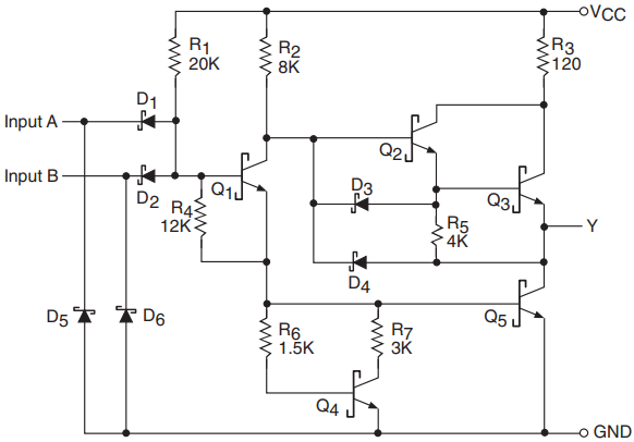
The multi-emitter input transistor is replaced by two PNP transistors Q1A and Q1B. Diodes D1A and D1B provide input clamping to negative excursions. Buffering offered by Q1A or Q1B and Q2 reduces the LOW-level input current by a factor of (1 + hFE of Q1A).
HIGH-level output voltage is determined primarily by VCC, transistors Q6 and Q7 and resistors R4 and R7 and is typically (VCC −2) V. LOW-level output voltage is determined by the turn-on characteristics of Q5. Transistor Q5 gets sufficient base drive through R3 and a conducting Q3 whose base terminal in turn is driven by a conducting Q2 whenever either or both inputs are HIGH. Transistor Q4 provides active turn-off for Q5.
Characteristic Features: Characteristic features of this family are summarized as follows:
- VIH = 2 V; VIL = 0.8 V; IIH = 20 µA; IIL = 0.1 mA; VOH = (VCC −2) V; VOL = 0.5 V; IOH = 0.4 mA; IOL = 8 mA (74ALS) and 4 mA (54ALS); VCC = 4.5 – 5.5 V;
- propagation delay (for a load resistance of 500Ω , a load capacitance of 50 pF, VCC = 4.5 – 5.5 V and an ambient temperature of minimum to maximum) = 11 ns/16 ns (max.) for LOW-to-HIGH and 8 ns/13 ns for HIGH-to-LOW output transitions (74ALS/54ALS);
- worst-case noise margin = 0.3 V; fan-out = 20; ICCH (for all four gates) = 0.85 mA; ICCL (for all four gates) = 3 mA;
- operating temperature range = 0 – 70 °C (74-series) and −55 to +125 °C (54-series);
- speed–power product = 4.8 pJ; maximum flip-flop toggle frequency = 70 MHz.
Advanced Schottky TTL (74AS/54AS)
Figure 17 shows the internal schematic of an advanced Schottky TTL NAND gate. The circuit shown is that of one of the four gates inside a quad two-input NAND (type 74AS00 or 54AS00). Salient features of ALS-TTL and AS-TTL have been discussed at length in the preceding paragraphs.
As is obvious from the internal circuit schematic of the AS-TTL NAND gate, it has some additional circuits not found in ALS-TTL devices. These are added to enhance the throughput of AS-TTL family devices.
Transistor Q10 provides a discharge path for the base-collector capacitance of Q5. In the absence of Q10, a rising voltage across the output forces current into the base of Q5 through its base-collector capacitance, thus causing it to turn on. Transistor Q10 turns on through D9, thus keeping transistor Q5 in the cut-off state.
Characteristic Features: Characteristic features of this family are summarized as follows:
- VIH = 2 V; VIL = 0.8 V; IIH = 20µ A; IIL = 0.5 mA; VOH = (VCC−2) V; VOL = 0.5 V; IOH = 2 mA; IOL = 20 mA;
- VCC = 4.5 – 5.5 V; propagation delay (for a load resistance of 50Ω , a load capacitance of 50 pF,
- VCC = 4.5 – 5.5 V and an ambient temperature of minimum to maximum) = 4.5 ns/5 ns (max.) for LOW-to-HIGH and 4 ns/5 ns (max.) for HIGH-to-LOW output transitions (74AS/54AS);
- worst-case noise margin = 0.3 V; fan-out = 40; ICCH (for all four gates) = 3.2 mA; ICCL (for all four gates) = 17.4 mA;
- operating temperature range = 0 – 70 °C (74-series) and −55 to +125 °C (54-series);
- speed–power product = 13.6 pJ; maximum flip-flop toggle frequency = 200 MHz.
Fairchild Advanced Schottky TTL (74F/54F)
The Fairchild Advanced Schottky TTL family, commonly known as FAST logic, is similar to the AS-TTL family. Figure 18 shows the internal schematic of a Fairchild Advanced Schottky TTL NAND gate.
The circuit shown is that of one of the four gates inside a quad two-input NAND (type 74F00 or 54F00). The DTL kind of input with emitter follower configuration of Q1 provides a good base drive to Q2. The ‘Miller killer’ configuration comprising varactor diode D7, transistor Q6 and associated components speeds up LOW-to-HIGH transition.
During LOW-to-HIGH transition, voltage at the emitter terminal of Q3 begins to rise while Q5 is still conducting. Varactor diode D7 conducts, thus supplying base current to Q6. A conducting Q6 provides a discharge path for the charge stored in the base-collector capacitance of Q5, thus expediting its turn-off.
Characteristic Features: Characteristic features of this family are summarized as follows:
- VIH = 2 V; VIL = 0.8 V; IIH = 20µ A; IIL = 0.6 mA; VOH = 2.7 V; VOL = 0.5 V; IOH = 1 mA; IOL = 20 mA; VCC = 4.75–5.25 V (74F) and 4.5– 5.5 V (54F);
- propagation delay (a load resistance of 500Ω , a load capacitance of 50 pF and full operating voltage and temperature ranges) = 5.3 ns/7 ns (max.) for LOW-to-HIGH and 6 ns/6.5 ns (max.) for HIGH-to-LOW output transitions (74AS/54AS);
- worst-case noise margin = 0.3 V; fanout = 40; ICCH (for all four gates) = 2.8 mA; ICCL (for all four gates) = 10.2 mA;
- operating temperature range = 0 – 70 °C (74F-series) and −55 to +125 °C (54F-series);
- speed–power product = 10 pJ; maximum flip-flop toggle frequency = 125 MHz.
Floating and Unused Inputs
The floating input of TTL family devices behaves as if logic HIGH has been applied to the input. Such behaviour is explained from the input circuit of a TTL device.
When the input is HIGH, the input emitter-base junction is reverse biased and the current that flows into the input is the reverse-biased diode leakage current. The input diode will be reverse biased even when the input terminal is left unconnected or floating, which implies that a floating input behaves as if there were logic HIGH applied to it.
As an initial thought, we may tend to believe that it should not make any difference if we leave the unused inputs of NAND and AND gates as floating, as logic HIGH like behaviour of the floating input makes no difference to the logical behaviour of the gate, as shown in Figs 19(a) and (b).
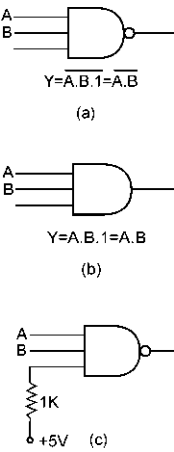
In spite of this, it is strongly recommended that the unused inputs of AND and NAND gates be connected to a logic HIGH input [Fig. 19(c)] because floating input behaves as an antenna and may pick up stray noise and interference signals, thus causing the gate to function improperly. 1 kΩ resistance is connected to protect the input from any current spikes caused by any spikes on the power supply line. More than one unused input (up to 50) can share the same 1 kΩ resistance, if needed.
In the case of OR and NOR gates, unused inputs are connected to ground (logic LOW), as shown in Fig. 20(c), for obvious reasons. A floating input or an input tied to logic HIGH in this case produces a permanent logic HIGH (for an OR gate) and LOW (for a NOR gate) at the output as shown in Figs 20(a) and (b) respectively.
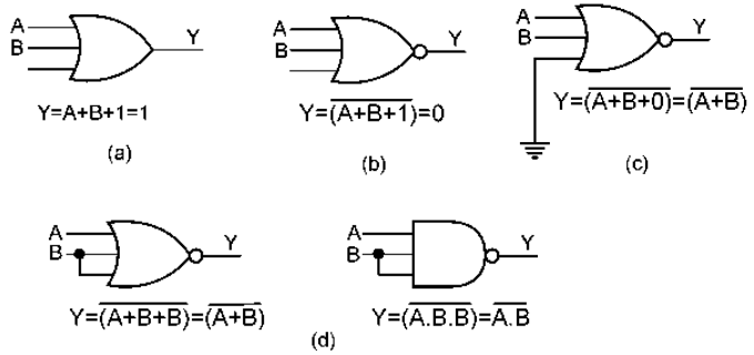
An alternative solution is shown in Fig. 20(d), where the unused input has been tied to one of the used inputs. This solution works well for all gates, but one has to be conscious of the fact that the fan-out capability of the output driving the tied inputs is not exceeded.
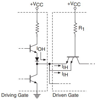
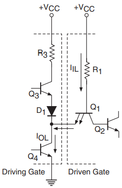
If we recall the internal circuit schematics of AND and NAND gates, we will appreciate that, when more than one input is tied together, the input loading, that is, the current drawn by the tied inputs from the driving gate output, in the HIGH state is n times the loading of one input (Fig. 21); n is the number of inputs tied together.
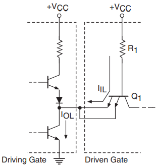
When the output is LOW, the input loading is the same as that of a single input. The reason for this is that, in the LOW input state, the current flowing out of the gate is determined by the resistance R1, as shown in Fig. 22.
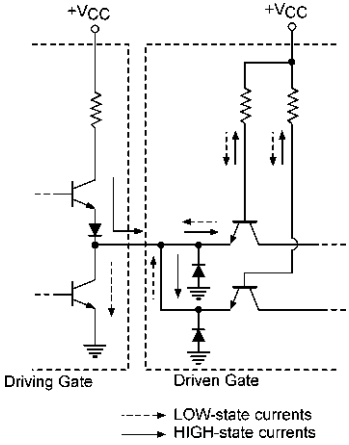
However, the same is not true in the case of OR and NOR gates, which do not use a multi-emitter input transistor and use separate input transistors instead, as shown in Fig. 23. In this case, the input loading is n times the loading of a single input for both HIGH and LOW states.
Current Transients and Power Supply Decoupling
TTL family devices are prone to occurrence of narrow-width current spikes on the power supply line. Current transients are produced when the totem-pole output stage of the device undergoes a transition from a logic LOW to a logic HIGH state.
The problem becomes severe when in a digital circuit a large number of gates are likely to switch states at the same time. These current spikes produce voltage spikes due to any stray inductance present on the line.
On account of the large rate of change in current in the current spike, even a small value of stray inductance produces voltage spikes large enough adversely to affect the circuit performance.
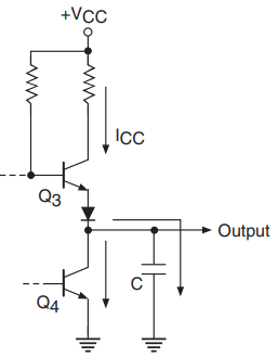
Figure 24 illustrates the phenomenon. When the output changes from LOW to HIGH, there is a small fraction of time when both the transistors are conducting because the pull-up transistor Q3 has switched on and the pull-down transistor Q4 has not yet come out of saturation. During this small fraction of time, there is an increase in current drawn from the supply; ICCL experiences a positive spike before it settles down to a usually lower ICCH.
The presence of any stray capacitance C across the output owing to any stray wiring capacitance or capacitance loading of the circuit being fed also adds to the problem.
The problem of voltage spikes on the power supply line is usually overcome by connecting small-value, low-inductance, high-frequency capacitors between VCC terminal and ground. It is standard practice to use a 0.01 or 0.1µ F ceramic capacitor from VCC to ground.
Related Posts
- Logic Gates
- Significance & Types of Logic Family
- Characteristics Parameters of Logic Families
- TTL Logic Family
- ECL Logic Family
- CMOS Logic Family
- Interfacing of Logic Families
- Microcontroller Architecture
- Components of Microcontroller
- Interfacing Devices with Microcontroller
- IC Based Multivibrator Circuits
- Astable, Monostable & Bistable Multivibrator
- Logic Analyser
- Types of Oscilloscope
- Frequency Synthesizers
- Frequency Counter