A.C. FROM D.C. SP – SP INVERSION
The business of getting a.c. from d.c. is known as inversion, and nine times out of ten we would ideally like to be able to produce sinusoidal output voltages of whatever frequency and amplitude we choose.
Unfortunately the constraints imposed by the necessity to use a switching strategy means that we always have to settle for a voltage waveform which is composed of rectangular chunks, and is thus far from ideal. Nevertheless it turns out that a.c. motors are remarkably tolerant, and will operate satisfactorily despite the inferior waveforms produced by the inverter.
Single-Phase Inverter
We can illustrate the basis of inverter operation by considering the single-phase example shown in Figure 1. This inverter uses bipolar transistors as the switching elements, with diodes (not shown) to provide the freewheel paths needed when the load is inductive.
The input or d.c. side of the inverter (on the left in Figure 1) is usually referred to as the ‘d.c. link’, reflecting the fact that in the majority of cases the d.c. is obtained by rectifying the incoming constant-frequency mains. The output or a.c. side is taken from terminals A and B as shown in Figure 1.
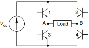
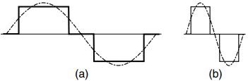
When transistors 1 and 4 are switched on, the load voltage is positive, and equal to the d.c. link voltage, while when 2 and 3 are on it is negative. If no devices are switched on, the output voltage is zero. Typical output voltage waveforms at low and high switching frequencies are shown in Figure 2(a) and (b), respectively.
Here each pair of devices is on for one-third of a cycle, and all the devices are off for two periods of one-sixth of a cycle. The output waveform is clearly not a sine wave, but at least it is alternating and symmetrical. The fundamental component is shown dotted in Figure 2.
Within each cycle the pattern of switching is regular, and easily programmed using appropriate logic circuitry. Frequency variation is obtained by altering the clock frequency controlling the four-step switching pattern. (The oscillator providing the clock signal can be controlled by an analogue voltage, or it can be generated using software.)
The effect of varying the switching frequency is shown in Figure 2, from which we can see that the amplitude of the fundamental component of voltage remains constant, regardless of frequency.
Unfortunately, this is not what we want for supplying an induction motor: to prevent the air-gap flux in the motor from falling as the frequency is raised we need to be able to increase the voltage in proportion to the frequency. We will look at voltage control shortly, after a brief digression to discuss the problem of ‘shoot-through’.
Inverters with the configurations shown in Figures 1 and 4 are subject to a potentially damaging condition which can arise if both transistors in one ‘leg’ of the inverter inadvertently turn on simultaneously.
This should never happen if the devices are switched correctly, but if something goes wrong and both devices are on together – even for a very short time – they form a short-circuit across the d.c. link. This fault condition is referred to as ‘shoot-through’ because a high current is established very rapidly, destroying the devices.
A good inverter there-fore includes provision for protecting against the possibility of shoot-through, usually by imposing a minimum time-delay between one device in the leg going off and the other coming on.
Output Voltage Control
There are two ways in which the amplitude of the output voltage can be controlled. First, if the d.c. link is provided from a.c. mains via a controlled rectifier or from a battery via a chopper, the d.c. link voltage can be varied. We can then set the amplitude of the output voltage to any value within the range of the link.
For a.c. motor drives we can arrange for the link voltage to track the output frequency of the inverter, so that at high output frequency we obtain a high output voltage and vice-versa. This method of voltage control results in a simple inverter, but requires a controlled (and thus relatively expensive) rectifier for the d.c. link.
The second method, which predominates in small and medium sizes, achieves voltage control by pulse-width-modulation (PWM) within the inverter itself. A cheaper uncontrolled rectifier can then be used to provide a constant-voltage d.c. link.
The principle of voltage control by PWM is illustrated in Figure 3. At low-output frequencies, a low-output voltage is usually required, so one of each pair of devices is used to chop the voltage, the mark– space ratio being varied to achieve the desired voltage at the output. The low fundamental voltage component at low frequency is shown dotted in Figure 3(a).
At a higher frequency a higher voltage is needed, so the chopping device is allowed to conduct for a longer fraction of each cycle, giving the higher fundamental output as shown in Figure 2.15(b). As the frequency is raised still higher, the separate ‘on’ periods eventually merge, giving the waveform as shown in Figure 3(c). Any further increase in frequency takes place without further increase in the output voltage, as shown in Figure 3(d).
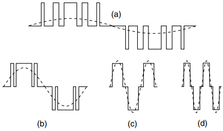
In drives applications, the range of frequencies over which the voltage/frequency ratio can be kept constant is known as the ‘PWM’ region, and the upper limit of the range is usually taken to define the ‘base speed’ of the motor.
Above this frequency, the inverter can no longer match voltage to frequency, the inverter effectively having run out of steam as far as voltage is concerned. The maximum voltage is thus governed by the link voltage, which must therefore be sufficiently high to provide whatever fundamental voltage the motor needs at its base speed, which is usually 50 or 60 Hz.
Beyond the PWM region the voltage waveform is as shown in Figure 3(d): this waveform is usually referred to as ‘quasi-square’, though in the light of the overall object of the exercise (to approximate to a sine wave) a better description might be ‘quasi-sine’.
When supplying an inductive motor load, fast recovery freewheel diodes are needed in parallel with each device. These may be discrete devices, or fitted in a common package with the transistor, or even integrated to form a single transistor/diode device.
Sinusoidal PWM
So far we have emphasised the importance of being able to control the amplitude of the fundamental output voltage by modulating the width of the pulses which make up the output waveform. If this was the only requirement, we would have an infinite range of modulation patterns which would be sufficient.
But as well as the right fundamental amplitude, we want the harmonic content to be minimised, i.e. we want the output waveform to be as close as possible to a pure sine wave. It is particularly important to limit the amplitude of the low-order harmonics, since these are the ones which are most likely to provoke an unwanted response from the motor.
The number, width, and spacing of the pulses is therefore optimised to keep the harmonic content as low as possible. A host of sophisticated strategies have been developed, almost all using a microprocessor-based system to store and/or generate the modulation patterns.
There is an obvious advantage in using a high switching frequency, since there are then more pulses to play with. Ultrasonic frequencies are now widely used, and as devices improve the switching frequencies continue to rise.
Most manufacturers claim their particular system is better than the competition, but it is not clear which will ultimately emerge as best for motor operation. Some early schemes used comparatively few pulses per cycle, and changed the number of pulses in discrete steps rather than smoothly, which earned them the nickname ‘gear-changers’. These inverters were noisy and irritating.
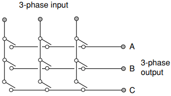
3-Phase Inverter
A 3-phase output can be obtained by adding only two more switches to the four needed for a single-phase inverter, giving the typical power circuit configuration shown in Figure 4. As usual, a freewheel diode is required in parallel with each transistor to protect against over-voltages caused by an inductive (motor) load.
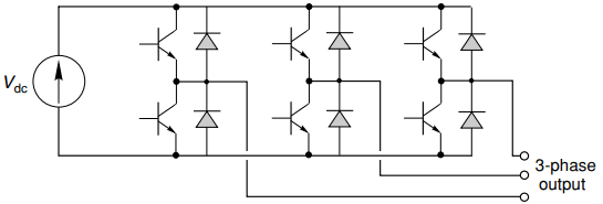
We note that the circuit configuration in Figure 4 is the same as for the 3-phase controlled rectifier looked at earlier. We mentioned then that the controlled rectifier could be used to regenerate, i.e. to convert power from d.c. to a.c., and this is of course ‘inversion’ as we now understand it.
Forced and Natural Commutation – Historical Perspective
We have assumed in this discussion that the switching devices can turnoff or ‘commutate’ on demand, so that the output (load) current is either reduced to zero or directed to another leg of the inverter. Transistors and gate-turn-off thyristors can operate like this, but, as explained earlier, conventional thyristors cannot turn off on command.
There are two distinct ways in which thyristors are used in inverters. In the first, where the inverter is used to supply an essentially passive a.c. load, such as an induction motor, each thyristor has to be equipped with its own auxiliary ‘forced commutating’ circuit, whose task is to force the current through the thyristor to zero when the time comes for it to turn off.
The commutating circuits are quite complex, and require substantial capacitors to store the energy required for commutation. Force-commutated thyristor converters therefore tend to be bulky and expensive. At one time they were the only alternative, but they are now more or less obsolete, having been superseded by MOSFET, IGBT or GTO versions.
The other way in which thyristors can be used to invert power from d.c. to a.c. is when the a.c. side of the bridge is connected to a three-phase stiff (i.e. low source impedance) mains supply. This is the normal ‘controlled rectifier’ arrangement introduced earlier.
In this case it turns out that the currents in the thyristors are naturally forced to zero by the active mains voltages, thereby allowing the thyristors to commutate or turn off naturally. This mode of operation continues to be important, as we will see when we look at d.c.motor drives.
Matrix Converters
Each of the converters we have looked at so far has been developed with a specific function in mind (e.g. rectifying a.c. to obtain d.c.), but they share an important common feature in that they all involve the use of sequentially operated switching devices to connect the output terminals to the supply terminals.
In all of these circuits the switching devices (transistors, thyristors, and diodes) can only conduct current in one direction, and this results in limitations on the ability of the circuit to operate with reverse power flow: for some circuits, e.g. the simple diode rectifier, reverse power flow is not possible at all.
The ideal power-electronic converter would allow power conversion in either direction between two systems of any voltage and frequency, including d.c., and would not involve any intermediate stage, such as a d.c. link.
In principle this can be achieved by means of an array of switches that allow any one of a set of input terminals to be connected to any one of a set of output terminals, at any desired instant.
Not surprisingly, the generic name for such converters is ‘matrix converter’. By way of example, Figure 5 shows nine switches arranged to permit power conversion between two three-phase systems.
The operation can best be understood by imagining that the input voltage is that of the sinusoidal three-phase mains system, so at every instant we know exactly what each incoming line-to-line voltage will be.
Let us assume that we wish to synthesise a three-phase sinusoidal output of a known voltage and frequency. At every instant we know what voltage we want, say between the lines A and B, and we know what the voltages are between the three incoming lines.
So we switch on whichever pair of the A and B switches connects us to the two incoming lines whose voltage at the time is closest to the desired output line-to-line voltage, and we stay with it while it offers the best approximation to what we want. When a different combination of switches would allow us to hook onto a more appropriate pair of input lines, the switching pattern changes.
A little thought will make clear that since at any instant there are only three different incoming line-to-line voltages to choose from, we cannot expect to synthesise a decent sinusoidal waveform with this sort of discrete switching, although this is the approach taken to derive a low-frequency output in the cycloconverter drive.
To obtain a better approximation to a sinusoidal waveform we must use chopping, where we switch rapidly on and off to modulate the output voltage amplitude. This means that the switches have to be capable of operating at much higher frequencies than the fundamental output frequency, so that switching loss becomes an important consideration.
In order for such converters to be able to transmit power in either direction (so that the terms input and output cease to have specific meanings), the switches (shown in Figure 5) must be capable of carrying current in either direction.
The lack of single affordable devices with this bi-directional current capability explains why matrix converters are not yet significant in the drives market, but their development is attracting attention and they look likely to emerge as improved control strategies and bi-directional switching devices become more practicable.
CONVERTER WAVEFORMS AND ACOUSTIC NOISE
In common with most textbooks, the waveforms shown in this chapter (and later in the book) are what we would hope to see under ideal conditions. It makes sense to concentrate on these ideal waveforms from the point of view of gaining a basic understanding, but we ought to be warned that what we see on an oscilloscope may well look rather different!
We have seen that the essence of power electronics is the switching process, so it should not come as much of a surprise to learn that in practice the switching is seldom achieved in such a clear-cut fashion as we have assumed.
Usually, there will be some sort of high-frequency oscillation or ‘ringing’ evident, particularly on the voltage waveforms following each transition due to switching.
This is due to the effects of stray capacitance and inductance: it should be anticipated at the design stage, and steps should be taken to minimise it by fitting ‘snubbing’ circuits at the appropriate places in the converter.
However complete suppression of all these transient phenomena is seldom economically worthwhile so the user should not be too alarmed to see remnants of the transient phenomena in the output waveforms.
Acoustic noise is also a matter which can worry newcomers. Most power electronic converters emit whining or humming sounds at frequencies corresponding to the fundamental and harmonics of the switching frequency, though when the converter is used to feed a motor, the sound from the motor is usually a good deal louder than the sound from the converter itself.
These sounds are very difficult to describe in words, but typically range from a high-pitched hum through a whine to a piercing whistle. They vary in intensity with the size of converter and the load, and to the trained ear can give a good indication of the health of the motor and converter.