Electronic Converters for Motor Drives
In this article we look at examples of the power converter circuits which are used with motor drives, providing either d.c. or a.c. outputs, and working from either a d.c. (battery) supply, or from the conventional a.c. mains. The treatment is not intended to be exhaustive, but should serve to highlight the most important aspects which are common to all types of drive converters.
Although there are many different types of converters, all except very low-power ones are based on some form of electronic switching. The need to adopt a switching strategy is emphasised in the first example, where the consequences are explored in some depth.
We will see that switching is essential in order to achieve high-efficiency power conversion, but that the resulting waveforms are inevitably less than ideal from the point of view of the motor. The examples have been chosen to illustrate typical practice, so for each converter the most commonly used switching devices (e.g. thyristor, transistor) are shown.
In many cases, several different switching devices may be suitable, so we should not identify a particular circuit as being the exclusive preserve of a particular device. Before discussing particular circuits, it will be useful to take an overall look at a typical drive system, so that the role of the converter can be seen in its proper context.
General Arrangement of Drives
A complete drive system is shown in block diagram form in Figure 1. The job of the converter is to draw electrical energy from the mains (at motor at whatever voltage and frequency necessary to achieve the desired mechanical output.
Except in the simplest converter (such as a simple diode rectifier), there are usually two distinct parts to the converter. The first is the power stage, through which the energy flows to the motor, and the second is the control section, which regulates the power flow.
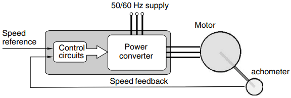
Control signals, in the form of low-power analogue or digital voltages, tell the converter what it is supposed to be doing, while other low-power feedback signals are used to measure what is actually happening. By comparing the demand and feedback signals, and adjusting the output accordingly, the target output is maintained.
The simple arrangement shown in Figure 1 has only one input representing the desired speed, and one feedback signal indicating actual speed, but most drives will have extra feedback signals as we will see later.
A characteristic of power electronic converters which is shared with most electrical systems is that they have very little capacity for storing energy. This means that any sudden change in the power supplied by the converter to the motor must be reflected in a sudden increase in the power drawn from the supply.
In most cases this is not a serious problem, but it does have two drawbacks. Firstly, a sudden increase in the current drawn from the supply will cause a momentary drop in the supply voltage, because of the effect of the supply impedance. These voltage ‘spikes’ will appear as unwelcome distortion to other users on the same supply. And secondly, there may be an enforced delay before the supply can furnish extra power.
With a single-phase mains supply, for example, there can be no sudden increase in the power supply from the mains at the instant where the mains voltage is zero, because instantaneous power is necessarily zero at this point in the cycle because the voltage is itself zero.
It would be better if a significant amount of energy could be stored within the converter itself: short-term energy demands could then be met instantly, thereby reducing rapid fluctuations in the power drawn from the mains. But unfortunately this is just not economic: most converters do have a small store of energy in their smoothing inductors and capacitors, but the amount is not sufficient to buffer the supply sufficiently to shield it from anything more than very short-term fluctuations.
VOLTAGE CONTROL – D.C. OUTPUT FROM D.C. SUPPLY
For the sake of simplicity we will begin by exploring the problem of controlling the voltage across a 2 V resistive load, fed from a 12 V constant-voltage source such as a battery. Three different methods are shown in Figure 2, in which the circle on the left represents an ideal 12 V d.c. source, the tip of the arrow indicating the positive terminal. Although this setup is not quite the same as if the load was a d.c. motor, the conclusions which we draw are more or less the same.
Method (a) uses a variable resistor (R) to absorb whatever fraction of the battery voltage is not required at the load. It provides smooth (albeit manual) control over the full range from 0 to 12 V, but the snag is that power is wasted in the control resistor.
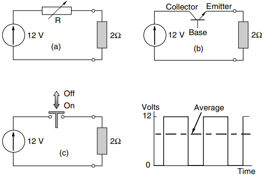
For example, if the load voltage is to be reduced to 6 V, the resistor (R) must be set to 2 V, so that half of the battery voltage is dropped across R. The current will be 3 A, the load power will be 18 W, and the power dissipated in R will also be 18 W.
In terms of overall power conversion efficiency (i.e. useful power delivered to the load divided by total power from the source) the efficiency is a very poor 50%. If R is increased further, the efficiency falls still lower, approaching zero as the load voltage tends to zero. This method of control is therefore unacceptable for motor control, except perhaps in low-power applications such as model racing cars.
Method (b) is much the same as (a) except that a transistor is used instead of a manually operated variable resistor. The transistor in Figure 2(b) is connected with its collector and emitter terminals in series with the voltage source and the load resistor. The transistor is a variable resistor, of course, but a rather special one in which the effective collector-emitter resistance can be controlled over a wide range by means of the base–emitter current.
The base–emitter current is usually very small, so it can be varied by means of a low-power electronic circuit (not shown in Figure 2) whose losses are negligible in comparison with the power in the main (collector-emitter) circuit.
Method (b) shares the drawback of method (a) above, i.e. the efficiency is very low. But even more seriously as far as power control is concerned, the ‘wasted’ power (up to a maximum of 18 W in this case) is burned off inside the transistor, which therefore has to be large, well-cooled, and hence expensive. Transistors are never operated in this ‘linear’ way when used in power electronics, but are widely used as switches, as discussed below.
Switching Control
The basic ideas underlying a switching power regulator are shown by the arrangement in Figure 2(c), which uses a mechanical switch. By operating the switch repetitively and varying the ratio of on/off time, the average load voltage can be varied continuously between 0 V (switch off all the time) through 6 V (switch on and off for half of each cycle) to 12 V (switch on all the time). The circuit shown in Figure 2(c) is often referred to as a ‘chopper’, because the battery supply is ‘chopped’ on and off.
When a constant repetition frequency is used, and the width of the on pulse is varied to control the mean output voltage (see the waveform in Figure 2), the arrangement is known as ‘pulse width modulation’ (PWM).
An alternative approach is to keep the width of the on pulses constant, but vary their repetition rate: this is known as pulse frequency modulation (PFM). The main advantage of the chopper circuit is that no power is wasted, and the efficiency is thus 100%.
When the switch is on, current flows through it, but the voltage across it is zero because its resistance is negligible. The power dissipated in the switch is therefore zero. Likewise, when the switch is ‘off’ the current through it is zero, so although the voltage across the switch is 12 V, the power dissipated in it is again zero.
The obvious disadvantage is that by no stretch of imagination could the load voltage be seen as ‘good’ d.c.: instead it consists of a mean or ‘d.c.’ level, with a superimposed ‘a.c.’ component.
Bearing in mind that we really want the load to be a d.c. motor, rather than a resistor, we are bound to ask whether the pulsating voltage will be acceptable. Fortunately, the answer is yes, provided that the chopping frequency is high enough.
We will see later that the inductance of the motor causes the current to be much smoother than the voltage, which means that the motor torque fluctuates much less than we might suppose, and the mechanical inertia of the motor filters the torque ripples so that the speed remains almost constant, at a value governed by the mean (or d.c.) level of the chopped waveform.
Obviously a mechanical switch would be unsuitable, and could not be expected to last long when pulsed at high frequency. So, an electronic power switch is used instead. The first of many devices to be used for switching was the bipolar junction transistor (BJT), so we will begin by examining how such devices are employed in chopper circuits.
If we choose a different device, such as a metal oxide semiconductor field effect transistor (MOSFET) or an insulated gate bipolar transistor (IGBT), the detailed arrangements for turning the device on and off will be diVerent, but the main conclusions we draw will be much the same.
Transistor Chopper
As noted earlier, a transistor is effectively a controllable resistor, i.e. the resistance between collector and emitter depends on the current in the base–emitter junction. In order to mimic the operation of a mechanical switch, the transistor would have to be able to provide infinite resistance (corresponding to an open switch) or zero resistance (corresponding to a closed switch). Neither of these ideal states can be reached with a real transistor, but both can be closely approximated.
The transistor will be ‘off’ when the base–emitter current is zero. Viewed from the main (collector-emitter) circuit, its resistance will be very high, as shown by the region Oa in Figure 3.
Under this ‘cut-off’ condition, only a tiny current (Ic) can flow from the collector to the emitter, regardless of the voltage (Vce) between the collector and emitter. The power dissipated in the device will therefore be negligible, giving an excellent approximation to an open switch.
To turn the transistor fully ‘on’, a base–emitter current must be provided. The base current required will depend on the prospective collector–emitter current, i.e. the current in the load. The aim is to keep the transistor ‘saturated’ so that it has a very low resistance, corresponding to the region Ob in Figure 3.
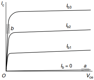
In the example shown in Figure 2, if the resistance of the transistor is very low, the current in the circuit will be almost 6 A, so we must make sure that the base– emitter current is sufficiently large to ensure that the transistor remains in the saturated condition when Ic = 6A.
Typically in a bipolar transistor (BJT) the base current will need to be around 5–10% of the collector current to keep the transistor in the saturation region: in the example (Figure 2), with the full load current of 6 A flowing, the base current might be 400 mA, the collector–emitter voltage might be say 0.33 V, giving an on-state dissipation of 2 W in the transistor when the load power is 72 W. The power conversion efficiency is not 100%, as it would be with an ideal switch, but it is acceptable.
We should note that the on-state base–emitter voltage is very low, which, coupled with the small base current, means that the power required to drive the transistor is very much less than the power being switched in the collector–emitter circuit.
Nevertheless, to switch the transistor in the regular pattern as shown in Figure 2, we obviously need a base current waveform which goes on and off periodically, and we might wonder how we obtain this ‘control’ signal.
Normally, the base-drive signal will originate from a low-power oscillator (constructed from logic gates, or on a single chip), or perhaps from a microprocessor.
Depending on the base circuit power requirements of the main switching transistor, it may be possible to feed it directly from the oscillator; if necessary additional transistors are interposed between the main device and the signal source to provide the required power amplification.
Just as we have to select mechanical switches with regard to their duty, we must be careful to use the right power transistor for the job in hand. In particular, we need to ensure that when the transistor is ‘on’, we don’t exceed the safe current, or else the active semiconductor region of the device will be destroyed by overheating.
And we must make sure that the transistor is able to withstand whatever voltage appears across the collector–emitter junction when it is ‘off’. If the safe voltage is exceeded, the transistor will breakdown, and be permanently ‘on’. A suitable heatsink will be a necessity.
Some heat is generated when the transistor is on, and at low switching rates this is the main source of unwanted heat. But at high switching rates, ‘switching loss’ can also be very important.
Switching loss is the heat generated in the finite time it takes for the transistor to go from on to off or vice versa. The base-drive circuitry will be arranged so that the switching takes place as fast as possible, but in practice it will seldom take less than a few microseconds.
During the switch ‘on’ period, for example, the current will be building up, while the collector–emitter voltage will be falling towards zero. The peak power reached can therefore be large, before falling to the relatively low on-state value.
Of course the total energy released as heat each time the device switches is modest because the whole process happens so quickly. Hence if the switching rate is low (say once every second) the switching power loss will be insignificant in comparison with the on-state power.
But at high switching rates, when the time taken to complete the switching becomes comparable with the on time, the switching power loss can easily become dominant.
In drives, switching rates from hundreds of hertz to the low tens of kilohertz are used: higher frequencies would be desirable from the point of view of smoothness of supply, but cannot be used because the resultant high switching loss becomes unacceptable.
Chopper with Inductive Load – Overvoltage Protection
So far we have looked at chopper control of a resistive load, but in a drives context the load will usually mean the winding of a machine, which will invariably be inductive.
Chopper control of inductive loads is much the same as for resistive loads, but we have to be careful to prevent the appearance of dangerously high voltages each time the inductive load is switched ‘off’.
The root of the problem lies with the energy stored in magnetic field of the inductor. When an inductance L carries a current I, the energy stored in the magnetic field (W) is given by
W = LI2 ÷ 2
If the inductor is supplied via a mechanical switch, and we open the switch with the intention of reducing the current to zero instantaneously, we are in effect seeking to destroy the stored energy. This is not possible, and what happens is that the energy is dissipated in the form of a spark across the contacts of the switch.
This sparking will be familiar to anyone who has pulled off the low-voltage lead to the ignition coil in a car. The appearance of a spark indicates that there is a very high voltage which is sufficient to breakdown the surrounding air.
We can anticipate this by remembering that the voltage and current in an inductance are related by the equation
V = L di/dt
The self-induced voltage is proportional to the rate of change of current, so when we open the switch in order to force the current to zero quickly, a very large voltage is created in the inductance.
This voltage appears across the terminals of the switch and if sufficient to breakdown the air, the resulting arc allows the current to continue to flow until the stored magnetic energy is dissipated as heat in the arc.
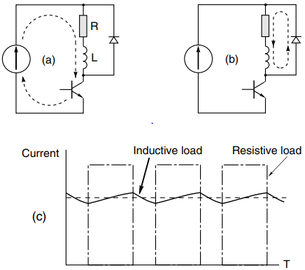
Sparking across a mechanical switch is unlikely to cause immediate destruction, but when a transistor is used sudden death is certain unless steps are taken to tame the stored energy. The usual remedy lies in the use of a ‘freewheel diode’ (sometimes called a flywheel diode), as shown in Figure 4.
A diode is a one-way valve as far as current is concerned: it offers very little resistance to current flowing from anode to cathode (i.e. in the direction of the broad arrow in the symbol for a diode), but blocks current flow from cathode to anode.
Actually, when a power diode conducts in the forward direction, the voltage drop across it is usually not all that dependent on the current flowing through it, so the reference above to the diode ‘offering little resistance’ is not strictly accurate because it does not obey Ohm’s law. In practice the volt-drop of power diodes (most of which are made from silicon) is around 0.7 V, regardless of the current rating.
In the circuit of Figure 4(a), when the transistor is on, current (I) flows through the load, but not through the diode, which is said to be reverse-biased (i.e. the applied voltage is trying unsuccessfully to push current down through the diode).
When the transistor is turned off, the current through it and the battery drops very quickly to zero. But the stored energy in the inductance means that its current cannot suddenly disappear.
So, since there is no longer a path through the transistor, the current diverts into the only other route available, and flows upwards through the low-resistance path offered by the diode, as shown in Figure 4(b). Obviously the current no longer has a battery to drive it, so it cannot continue to flow indefinitely.
In fact it will continue to ‘freewheel’ only until the energy originally stored in the inductance is dissipated as heat, mainly in the load resistance but also in the diode’s own (low) resistance.
The current waveform during chopping will then be as shown in Figure 4(c). Note that the current rises and falls exponentially with a time-constant of L/R, though it never reaches anywhere near its steady-state value in Figure 4.
The sketch corresponds to the case where the time-constant is much longer than one switching period, in which case the current becomes almost smooth, with only a small ripple.
In a d.c. motor drive this is just what we want, since any fluctuation in the current gives rise to torque pulsations and consequent mechanical vibrations. (The current waveform that would be obtained with no inductance is also shown in Figure 4: the mean current is the same but the rectangular current waveform is clearly much less desirable, given that ideally we would like constant d.c.)
Finally, we need to check that the freewheel diode prevents any dangerously high voltages from appearing across the transistor.
As explained above, when the diode conducts, the forward-bias volt-drop across it is small – typically 0.7 V. Hence while the current is freewheeling, the voltage at the collector of the transistor is only 0.7 V above the battery voltage.
This ‘clamping’ action therefore limits the voltage across the transistor to a safe value, and allows inductive loads to be switched without damage to the switching element.
Features of Power Electronic Converters
We can draw some important conclusions which are valid for all power electronic converters from this simple example. Firstly, efficient control of voltage (and hence power) is only feasible if a switching strategy is adopted. The load is alternately connected and disconnected from the supply by means of an electronic switch, and any average voltage up to the supply voltage can be obtained by varying the mark/space ratio.
Secondly, the output voltage is not smooth d.c., but contains unwanted a.c. components which, though undesirable, are tolerable in motor drives.
And finally, the load current waveform will be smoother than the voltage waveform if – as is the case with motor windings – the load is inductive.