D.C. FROM A.C. – CONTROLLED RECTIFICATION
The vast majority of drives of all types draw their power from constant voltage 50 or 60 Hz mains, and in nearly all mains converters the first stage consists of a rectifier which converts the a.c. to a crude form of d.c. Where a constant-voltage (i.e. unvarying average) ‘d.c.’ output is required, a simple (uncontrolled) diode rectifier is sufficient.
But where the mean d.c. voltage has to be controllable (as in a d.c. motor drive to obtain varying speeds), a controlled rectifier is used. Many different converter configurations based on combinations of diodes and thyristors are possible, but we will focus on ‘fully-controlled’ converters in which all the rectifying devices are thyristors. These are widely used in modern motor drives.
From the user’s viewpoint, interest centres on the following questions: .
- How is the output voltage controlled?
- What does the converter output voltage look like?
- Will there be any problem if the voltage is not pure d.c.?
- How does the range of the output voltage relate to a.c. mains voltage?
We can answer these questions without going too thoroughly into the detailed workings of the converter. This is just as well, because understanding all the ins and outs of converter operation is beyond our scope.
On the other hand it is well worth trying to understand the essence of the controlled rectification process, because it assists in understanding the limitations which the converter puts on drive performance.
Single-Pulse Rectifier
The simplest phase-controlled rectifier circuit is shown in Figure 1. When the supply voltage is positive, the thyristor blocks forward current until the gate pulse arrives, and up to this point the voltage across the resistive load is zero.
As soon as a firing pulse is delivered to the gate-cathode circuit (not shown in Figure 1) the device turns on, the voltage across it falls to near zero, and the load voltage becomes equal to the supply voltage.
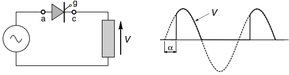
When the supply voltage reaches zero, so does the current. At this point the thyristor regains its blocking ability, and no current flows during the negative half-cycle.
If we neglect the small on-state volt-drop across the thyristor, the load voltage (Figure 1) will consist of part of the positive half-cycles of the a.c. supply voltage.
It is obviously not smooth, but is ‘d.c.’ in the sense that it has a positive mean value; and by varying the delay angle (α) of the firing pulses the mean voltage can be controlled.
The arrangement shown in Figure 1 gives only one peak in the rectified output for each complete cycle of the mains, and is therefore known as a ‘single-pulse’ or half-wave circuit.
The output voltage (which ideally we would want to be steady d.c.) is so poor that this circuit is never used in drives. Instead, drive converters use four or six thyristors, and produce much superior output waveforms with two or six pulses per cycle, as will be seen in the following sections.
Single-Phase Fully Controlled Converter – Output Voltage and Control
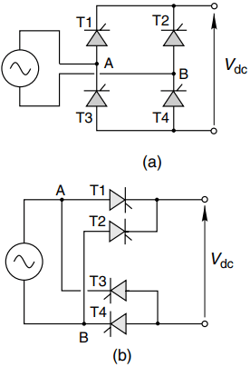
The main elements of the converter circuit are shown in Figure 2. It comprises four thyristors, connected in bridge formation. The conventional way of drawing the circuit is shown in Figure 2(a), while in Figure 2(b) it has been redrawn to assist understanding.
The top of the load can be connected (via T1) to terminal A of the mains, or (via T2) to terminal B of the mains, and likewise the bottom of the load can be connected either to A or to B via T3 or T4, respectively.
We are naturally interested to find what the output voltage waveform on the d.c. side will look like, and in particular to discover how the mean d.c. level can be controlled by varying the firing delay angle (α).
This is not as simple as we might have expected, because it turns out that the mean voltage for a given a depends on the nature of the load. We will therefore look first at the case where the load is resistive, and explore the basic mechanism of phase control. Later, we will see how the converter behaves with a typical motor load.
Resistive Load
Thyristors T1 and T4 are fired together when terminal A of the supply is positive, while on the other half-cycle, when B is positive, thyristors T2 and T3 are fired simultaneously. The output voltage waveform is shown by the solid line in Figure 3. There are two pulses per mains cycle, hence the description ‘two-pulse’ or full-wave.
At every instant the load is either connected to the mains by the pair of switches T1 and T4, or it is connected the other way up by the pair of switches T2 and T3, or it is disconnected.
The load voltage therefore consists of rectified chunks of the mains voltage. It is much smoother than in the single-pulse circuit, though again it is far from pure d.c. The waveforms in Figure 3 correspond to α = 45o and α = 135o respectively. The mean value, Vdc is shown in each case.
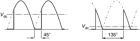
It is clear that the larger the delay angle, the lower the output voltage. The maximum output voltage (Vdo) is obtained with α = 0: this is the same as would be obtained if the thyristors were replaced by diodes, and is given by
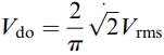
Where Vrms is the r.m.s. voltage of the incoming mains. The variation of the mean d.c. voltage with α is given by
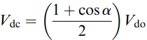
from which we see that with a resistive load the d.c. voltage can be varied from a maximum of Vdo down to zero by varying α from 0o to 180o.
Inductive (Motor) Load
As mentioned above, motor loads are inductive, and we have seen earlier that the current cannot change instantaneously in an inductive load. We must therefore expect the behaviour of the converter with an inductive load to differ from that with a resistive load, in which the current can change instantaneously.
The realisation that the mean voltage for a given firing angle might depend on the nature of the load is a most unwelcome prospect. What we would like to say is that, regardless of the load, we can specify the output voltage waveform once we have fixed the delay angle (α). We would then know what value of α to select to achieve any desired mean output voltage.
What we find in practice is that once we have fixed α, the mean output voltage with a resistive–inductive load is not the same as with a purely resistive load, and therefore we cannot give a simple general formula for the mean output voltage in terms of α.
This is of course very undesirable: if for example we had set the speed of our unloaded d.c. motor to the target value by adjusting the firing angle of the converter to produce the correct mean voltage, the last thing we would want is for the voltage to fall when the load current drawn by the motor increases, as this would cause the speed to fall below the target.
Fortunately however, it turns out that the output voltage waveform for a given α does become independent of the load inductance once there is sufficient inductance to prevent the load current from falling to zero. This condition is known as ‘continuous current’; and happily, many motor circuits do have sufficient self-inductance to ensure that we achieve continuous current.
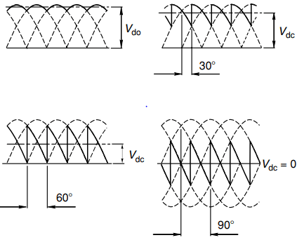
Under continuous current conditions, the output voltage waveform only depends on the firing angle, and not on the actual inductance present. This makes things much more straightforward, and typical output voltage waveforms for this continuous current condition are shown in Figure 4. The waveform in Figure 4(a) corresponds to α = 15, while Figure 4(b) corresponds to α = 60.
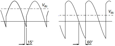
We see that, as with the resistive load, the larger the delay angle the lower the mean output voltage. However, with the resistive load the output voltage was never negative, whereas we see that for short periods the output voltage can now become negative. This is because the inductance smoothes out the current so that at no time does it fall to zero.
As a result, one pair of thyristors is always conducting, so at every instant the load is connected directly to the mains supply, and the load voltage always consists of chunks of the supply voltage.
It is not immediately obvious why the current switches over (or ‘commutates’) from the first pair of thyristors to the second pair when the latter are fired, so a brief look at the behaviour of diodes in a similar circuit configuration may be helpful at this point.
Consider the setup shown in Figure 5, with two voltage sources (each time-varying) supplying a load via two diodes. The question is what determines which diode conducts, and how does this influences the load voltage? We can consider two instants as shown in the diagram.
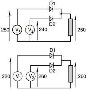
On the left, V1 is 250 V, V2 is 240 V, and D1 is conducting, as shown by the heavy line. If we ignore the volt-drop across the diode, the load voltage will be 250 V, and the voltage across diode D2 will be 240 – 250 = -10 V, i.e. it is reverse biased and hence in the non-conducting state.
At some other instant (on the right of the diagram), V1 has fallen to 220 V while V2 has increased to 260 V: now D2 is conducting instead of D1, again shown by the heavy line, and D1 is reverse-biased by -40 V.
The simple pattern is that the diode with the highest anode potential will conduct, and as soon as it does so it automatically reverse-biases its predecessor.
In a single-phase diode bridge, for example, the commutation occurs at the point where the supply voltage passes through zero: at this instant the anode voltage on one pair goes from positive to negative, while on the other pair the anode voltage goes from negative to positive.
The situation in controlled thyristor bridges is very similar, except that before a new device can takeover conduction, it must not only have a higher anode potential, but it must also receive a firing pulse. This allows the changeover to be delayed beyond the point of natural (diode) commutation by the angle α, as shown in Figure 4.
Note that the maximum mean voltage (Vdo) is again obtained when α is zero, and is the same as for the resistive load (equation 1). It is easy to show that the mean d.c. voltage is now related to α by
Vdc = Vdo cosα ( Equation 3)
This equation indicates that we can control the mean output voltage by controlling α, though equation 3 shows that the variation of mean voltage with α is different from that for a resistive load (equation 2).
We also see that when α is greater than 90o the mean output voltage is negative. The fact that we can obtain a nett negative output voltage with an inductive load contrasts sharply with the resistive load case, where the output voltage could never be negative.
We will see later that this facility allows the converter to return energy from the load to the supply, and this is important when we want to use the converter with a d.c. motor in the regenerating mode.
It is sometimes suggested (particularly by those with a light-current background) that a capacitor could be used to smooth the output voltage, this being common practice in cheap low-power d.c. supplies.
Although this works well at low power, there are two reasons why capacitors are not used with controlled rectifiers supplying motors. Firstly, it is not necessary for the voltage to be smooth as it is the current which directly determines the torque, and as already pointed out the current is always much smoother than the voltage because of inductance.
And secondly, the power levels in most drives are such that in order to store enough energy to smooth out the rectified voltage, very bulky and expensive capacitors would be required.
3-Phase Fully Controlled Converter
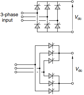
The main power elements are shown in Figure 6. The three-phase bridge has only two more thyristors than the single-phase bridge, but the output voltage waveform is vastly better, as shown in Figure 7. There are now six pulses of the output voltage per mains cycle, hence the description ‘six-pulse’.
The thyristors are again fired in pairs (one in the top half of the bridge and one – from a different leg – in the bottom half), and each thyristor carries the output current for one third of the time.
As in the single-phase converter, the delay angle controls the output voltage, but now α = 0 corresponds to the point at which the phase voltages are equal (see Figure 7).
The enormous improvement in the smoothness of the output voltage waveform is clear when we compare Figure 4 and Figure 7 , and it indicates the wisdom of choosing a 3-phase converter whenever possible.
The very much better voltage waveform also means that the desirable ‘continuous current’ condition is much more likely to be met, and the waveforms in Figure 7 have therefore been drawn with the assumption that the load current is in fact continuous.
Occasionally, even a sixpulse waveform is not sufficiently smooth, and some very large drive converters therefore consist of two six-pulse converters with their outputs in series. A phase-shifting transformer is used to insert a 30o shift between the a.c. supplies to the two 3-phase bridges. The resultant ripple voltage is then 12-pulse.
Returning to the six-pulse converter, the mean output voltage can be shown to be given by
We note that we can obtain the full range of output voltages from +Vdo to -Vdo, so that, as with the single-phase converter, regenerative operation will be possible.
It is probably a good idea at this point to remind the reader that, our interest in the controlled rectifier is as a supply to the armature of a d.c. motor.
When we examine the d.c. motor drive, we will see that it is the average or mean value of the output voltage from the controlled rectifier that determines the speed, and it is this mean voltage that we refer to when we talk of ‘the voltage’ from the converter. We must not forget the unwanted a.c. or ripple element, however, as this can be large.
For example, we see from Figure 7 that to obtain a very low voltage (to make the motor run very slowly) a will be close to zero; but if we were to connect an a.c. voltmeter to the output terminals it could register several hundred volts, depending on the incoming mains voltage!
Output Voltage Range
Mains a.c. supply voltages obviously vary around the world, but single-phase supplies are usually 220–240 V, and we see from equation 1 that the maximum mean d.c. voltage available from a single-phase 240 V supply is 216 V. This is suitable for 180–200 V motors. If a higher voltage is needed (say for a 300 V motor), a transformer must be used to step up the mains.
Turning now to typical three-phase supplies, the lowest three-phase industrial voltages are usually around 380–440 V. So with Vrms = 415 V for example, the maximum d.c. output voltage (equation 4) is 560 V.
After allowances have been made for supply variations and impedance drops, we could not rely on obtaining much more than 520–540 V, and it is usual for the motors used with six-pulse drives fed from 415 V, three-phase supplies to be rated in the range 440–500 V.
Often the motor’s field winding will be supplied from single-phase 240 V, and field voltage ratings are then around 180–200 V, to allow a margin in hand from the theoretical maximum of 216 V referred to earlier.
Firing Circuits
Since the gate pulses are only of low power, the gate drive circuitry is simple and cheap. Often a single integrated circuit (chip) contains all the circuitry for generating the gate pulses, and for synchronising them with the appropriate delay angle (α) with respect to the supply voltage.
To avoid direct electrical connection between the high voltages in the main power circuit and the low voltages used in the control circuits, the gate pulses are usually coupled to the thyristor by means of small pulse transformers.
Most converters also include what is known as ‘inverse cosine-weighted’ firing circuitry: this means that the firing circuit is so arranged that the ‘cosine’ relationship is incorporated internally so that the mean output voltage of the converter becomes directly proportional to the input control voltage, which typically ranges from 0 to 10 V.