Enhancement Type MOSFETs
In this type of MOSFET, channel is formed after applying biasing hence it is named as enhancement type. This MOSFET is smaller in size, economical and provides better performance than depletion MOSFET.
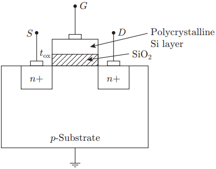
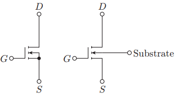
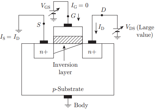
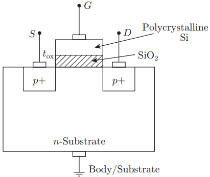
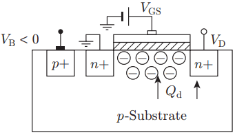
Figures 1(a) and (b) depict the cross-sectional view and circuit symbols of n-channel enhancement type MOSFET, respectively.
The broken line in the symbol indicates the absence of a channel.
Here the Al plate is replaced by polycrystalline Si material. The source and drain are kept apart as there is no channel existing in between source and drain region.
In this MOSFET, the channel is created by applying proper VGS. When positive gate to source voltage is applied, electron starts accumulating under gate; hence channel is formed.
Since p-substrate is converted to n-channel due to accumulation of electrons under the gate; it is also called inversion layer. The channel is also called induced channel.
The MOSFET acts as a capacitor which is formed because of positive metal plate (polycrystalline silicon), negative inversion layer and a SiO2 dielectric sandwiched between them, when a positive drain to source voltage is applied. A high intensity electric field is produced and electrons start moving from source to drain.
Operation of Enhancement Type n-Channel MOSFET
Figure 2 shows the construction and working of n-channel enhancement MOSFET.
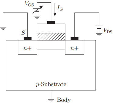
1. If drain terminal is kept floating, no current will be passing through the channel, that is, ID = 0. Thus the MOSFET does not conduct when VGS = 0 because there is no channel available for flow of drain current. The MOSFET is now working as a parallel plate capacitor.
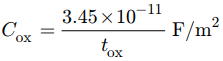
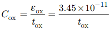
For the MOS capacitor, the oxide capacitance (Cox) per unit cross sectional area is given by
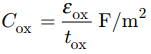
Where εox is permittivity in F/m and given by εox = ε0 εr
For SiO2, ε0 is absolute permittivity of for free space = 8.854 × 10⁻¹² and εr = relative permittivity = 3.9.
Therefore, ε0 εr = 8.854 × 3.9 × 10−12 = 3.45 × 10⁻¹¹ F/m
Gate capacitance is given by Cgate = CoxWL Farad
Where L is the length of the gate plate or channel and W is the width of the gate plate.
W/L > 1.
W/L Ratio is called aspect ratio per feature size.
2. The drain current can pass through the MOSFET only when VDS is applied. The circuit for n-channel enhancement type MOSFET when VDS is applied is shown in Fig. 3(a).
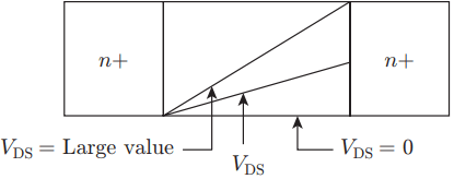
When VDS is kept at zero, the diode is unbiased and in the absence of depletion layer the channel will remain flat. When VDS is large, the diode is reverse biased at the drain, depletion layer will penetrate more into substrate tapering the channel and due to high electric field current becomes constant. This is depicted in Fig. 3(b).
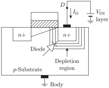
When VDS is of large value, a p-n junction is formed at drain and gets reverse biased and depletion layer is increased as shown in Fig. 4.
3. The discontinuity of the channel can be avoided by connecting substrate voltage VSB or body voltage.
When VDS is increasing, the channel length decreases and this whole process where the length of the channel can be altered by varying VDS is called the channel length modulation (CLM). CLM effect occurs only in enhancement MOSFET.
Due to CLM, EMOSFETs cannot be operated with self-biased arrangement or potential divider bias circuit.
Some important points related to n-channel enhancement type MOSFET are:
- Channel potential increases from source to drain.
- Inversion charges decrease from source to drain.
- When VGS = 0, ID = 0.
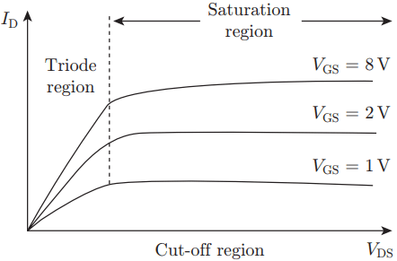
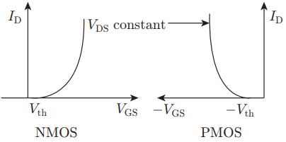
The transfer and drain characteristics of n-channel enhancement MOSFET are shown in Fig. 5(a) and (b).
From the transfer characteristic curve, we have for Vth as the threshold voltage:
- If VGS < Vth MOSFET is in OFF state
- When VGS > Vth MOSFET is in ON state
From the drain characteristic curves, we have:
- When VDS = VGS — Vth or VDS > VGS — Vth, the MOSFET is operating in the saturation region.
- When VDS < VGS — Vth, the MOSFET operates in linear region VDS < VDS(sat)
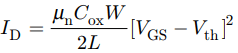
- Equation for drain current in saturation region is
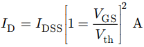
Where VGS >> Vth
Some important relations for n-channel enhancement type MOSFET
When VGS < Vth; ID = 0; cut-off region.
When VDS < VGS — Vth; ID = linear current; linear/ triode region. Drain current is given by
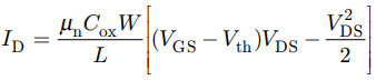
When VDS ≥ VGS — Vth; ID = saturation current; saturation region. Drain current is given by
Operation of Enhancement Type p-Channel MOSFET
The p-channel enhancement type MOSFET is similar in construction and operation to n-channel enhancement type MOSFET.

Figures 6(a) and (b) show the cross-sectional view and the circuit symbols for p-channel E-MOSFET.
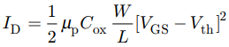
Some important relations for p-channel E-MOSFETs
When VGS > VT ; ID = 0; cut-off region
When VDS ≥ VGS — VT ; ID is linear; active/linear/triode region. Drain current is given by
When VDS < VGS — Vth; ID is constant; saturation region. The drain current is given by
The characteristics of depletion and enhancement MOSFETs are compared in following Table.
| Depletion Type | Enhancement Type |
| Pre-existing/diffused channel is available. | There is no pre-existing channel. Channel has to be created after applying VGS |
| Diffused channel | Induced channel |
| Suitable to operate in depletion and enhancement mode | Suitable only for saturation mode |
| When VGS = 0, ID = IDSS | When VGS = 0, ID = 0 |
| No channel length modulation | CLM effect exists |
| Continuous/uniform/flat channel | Discontinuous/tapered channel |
| Larger in size and expensive due to aluminium layer | Smaller in size and economical and better performance due to polycrystalline silicon layer |
| Can be designed in self-bias arrangement | Cannot be arranged in self-bias |
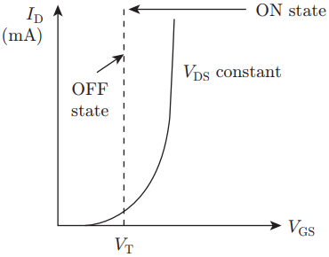
Threshold Voltage
Threshold voltage (Vth) is the minimum gate to source voltage at which conduction starts in a MOSFET. It can be graphically obtained from the transfer characteristics of MOSFET and appears only in enhancement type MOSFETs as shown in Fig. 7.
The voltage at which the MOSFET enters into ON state:
- Vth is positive for n-channel MOSFET
- Vth is negative for p-channel MOSFET
The value of Vth lies in the range 0.5 V to 3 V (typical value 1V). Vth must be small for better performance of MOSFET. The advantages of its small value are listed as follows:
- Enables the device to operate with smaller supply voltages.
- Increases the compatibility of device.
- Reduces switching time of devices so that they become faster in operation.
The threshold voltage for n-channel E-MOSFET is given by
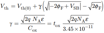
Where:
γ is fabrication process parameter.
φF is physical parameter of Fermi voltage.
VSB is substrate voltage or body voltage.
NA is accepter concentration or doping concentration of p-type substrate in n-channel MOSFET.
Vth(0) is threshold voltage of MOSFET when substrate voltage is kept zero (VSB = 0)
From the equation for threshold voltage, we have Vth α VSB
Normally body and the source are tied to the ground. If body voltage (VB) drops below the source voltage, VSB increases. If VB becomes more negative, more holes are attracted towards body connection leaving a larger negative charge behind.
Hence, the depletion region becomes wider. Thus, Vth is the function of total change in the depletion region.
As VB decreases, depletion region increases and threshold voltage increases. This is called body effect or back gate effect or substrate bias effect and is depicted in Fig. 8.
The threshold voltage of MOSFET can be reduced by using any one of the following methods:
- Reducing the doping concentration of substrate material.
- Increasing Cox.
- Reducing toxx2 .
- Using implantation techniques.
- Replacing Al plate with polycrystalline silicon.