CMOS Logic Family
The CMOS (Complementary Metal Oxide Semiconductor) logic family uses both N-type and P-type MOSFETs (enhancement MOSFETs, to be more precise) to realize different logic functions. The two types of MOSFET are designed to have matching characteristics. That is, they exhibit identical characteristics in switch-OFF and switch-ON conditions.
The main advantage of the CMOS logic family over bipolar logic families discussed so far lies in its extremely low power dissipation, which is near-zero in static conditions. In fact, CMOS devices draw power only when they are switching. This allows integration of a much larger number of CMOS gates on a chip than would have been possible with bipolar or NMOS (to be discussed later) technology.
CMOS technology today is the dominant semiconductor technology used for making microprocessors, memory devices and application-specific integrated circuits (ASICs).
The CMOS logic family, like TTL, has a large number of subfamilies. The basic difference between different CMOS logic subfamilies such as 4000A, 4000B, 4000UB, 74C, 74HC, 74HCT, 74AC and 74ACT is in the fabrication process used and not in the design of the circuits employed to implement the intended logic function.
We will firstly look at the circuit implementation of various logic functions in CMOS and then follow this up with a brief description of different subfamilies of CMOS logic.
Circuit Implementation of Logic Functions
In the following paragraphs, we will briefly describe the internal schematics of basic logic functions when implemented in CMOS logic. These include inverter, NAND, NOR, AND, OR, EX-OR, EX-NOR and AND-OR-INVERT functions.
CMOS Inverter: The inverter is the most fundamental building block of CMOS logic. It consists of a pair of N-channel and P-channel MOSFETs connected in cascade configuration as shown in Fig. 1.
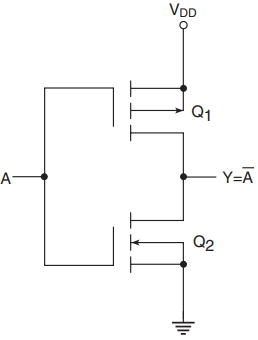
The circuit functions as follows. When the input is in the HIGH state (logic ‘1’), P-channel MOSFET Q1 is in the cut-off state while the N-channel MOSFET Q2 is conducting. The conducting MOSFET provides a path from ground to output and the output is LOW (logic ‘0’).
When the input is in the LOW state (logic ‘0’), Q1 is in conduction while Q2 is in cut-off. The conducting P-channel device provides a path for VDD to appear at the output, so that the output is in HIGH or logic ‘1’ state.
A floating input could lead to conduction of both MOSFETs and a short-circuit condition. It should therefore be avoided. It is also evident from Fig. 1 that there is no conduction path between VDD and ground in either of the input conditions, that is, when input is in logic ‘1’ and ‘0’ states.
That is why there is practically zero power dissipation in static conditions. There is only dynamic power dissipation, which occurs during switching operations as the MOSFET gate capacitance is charged and discharged. The power dissipated is directly proportional to the switching frequency.
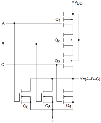
NAND Gate: Figure 2 shows the basic circuit implementation of a two-input NAND. As shown in the figure, two P-channel MOSFETs (Q1 and Q2) are connected in parallel between VDD and the output terminal, and two N-channel MOSFETs (Q3 and Q4) are connected in series between ground and output terminal.
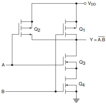
The circuit operates as follows. For the output to be in a logic ‘0’ state, it is essential that both the series-connected N-channel devices conduct and both the parallel-connected P-channel devices remain in the cut-off state. This is possible only when both the inputs are in a logic ‘1’ state. This verifies one of the entries of the NAND gate truth table.
When both the inputs are in a logic ‘0’ state, both the N-channel devices are non-conducting and both the P-channel devices are conducting, which produces a logic ‘1’ at the output. This verifies another entry of the NAND truth table.
For the remaining two input combinations, either of the two N-channel devices will be non-conducting and either of the two parallel-connected P-channel devices will be conducting. We have either Q3 OFF and Q2 ON or Q4 OFF and Q1 ON. The output in both cases is a logic ‘1’, which verifies the remaining entries of the truth table.
From the circuit schematic of Fig. 2 we can visualize that under no possible input combination of logic states is there a direct conduction path between VDD and ground. This further confirms that there is near-zero power dissipation in CMOS gates under static conditions.
Figure 3 shows how the circuit of Fig. 2 can be extended to build a three-input NAND gate. Operation of this circuit can be explained on similar lines.
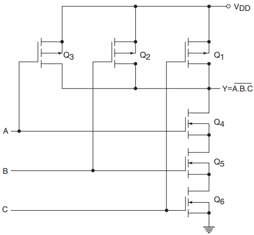
It may be mentioned here that series connection of MOSFETs adds to the propagation delay, which is greater in the case of P-channel devices than it is in the case of N-channel devices. As a result, the concept of extending the number of inputs as shown in Fig. 3 is usually limited to four inputs in the case of NAND and to three inputs in the case of NOR.
The number is one less in the case of NOR because it uses series-connected P-channel devices. NAND and NOR gates with larger inputs are realized as a combination of simpler gates.
NOR Gate: Figure 4 shows the basic circuit implementation of a two-input NOR. As shown in the figure, two P-channel MOSFETs (Q1 and Q2) are connected in series between VDD and the output terminal, and two N-channel MOSFETs (Q3 and Q4) are connected in parallel between ground and output terminal. The circuit operates as follows.
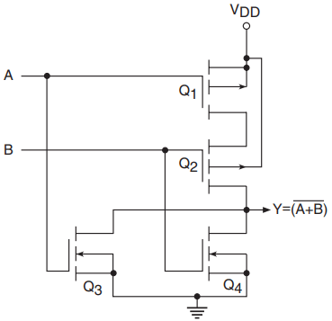
For the output to be in a logic ‘1’ state, it is essential that both the series-connected P-channel devices conduct and both the parallel-connected N-channel devices remain in the cut-off state. This is possible only when both the inputs are in a logic ‘0’ state. This verifies one of the entries of the NOR gate truth table.
When both the inputs are in a logic ‘1’ state, both the N-channel devices are conducting and both the P-channel devices are non-conducting, which produces a logic ‘0’ at the output. This verifies another entry of the NOR truth table.
For the remaining two input combinations, either of the two parallel N-channel devices will be conducting and either of the two series-connected P-channel devices will be non-conducting. We have either Q1 OFF and Q3 ON or Q2 OFF and Q4 ON. The output in both cases is logic ‘0’, which verifies the remaining entries of the truth table.
Figure 5 shows how the circuit of Fig. 4 can be extended to build a three-input NOR gate. The operation of this circuit can be explained on similar lines. As already explained, NOR gates with more than three inputs are usually realized as a combination of simpler gates.
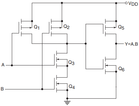
AND Gate: An AND gate is nothing but a NAND gate followed by an inverter. Figure 6 shows the internal schematic of a two-input AND in CMOS. A buffered AND gate is fabricated by using a NOR gate schematic with inverters at both of its inputs and its output feeding two series-connected inverters.
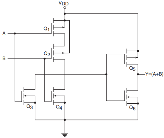
OR Gate: An OR gate is nothing but a NOR gate followed by an inverter. Figure 7 shows the internal schematic of a two-input OR in CMOS. A buffered OR gate is fabricated by using a NAND gate schematic with inverters at both of its inputs and its output feeding two series-connected inverters.
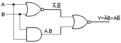
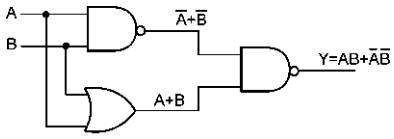
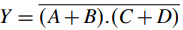
EXCLUSIVE-OR Gate: An EXCLUSIVE-OR gate is implemented using the logic diagram of Fig. 8(a). As is evident from the figure, the output of this logic arrangement can be expressed by

Figure 8(b) shows the internal schematic of a two-input EX-OR gate.
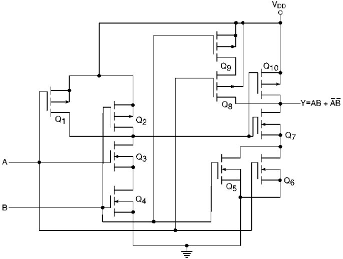
MOSFETs Q1–Q4 constitute the NOR gate. MOSFETS Q5 and Q6 simulate ANDing of A and B, and MOSFET Q7 provides ORing of the NOR output with ANDed output. Since MOSFETs Q8–Q10 make up the complement of the arrangement of MOSFETs Q5–Q7, the final output is inverted. Thus, the schematic of Fig. 8(b) implements the logic arrangement of Fig. 8(a) and hence a two-input EX-OR gate.
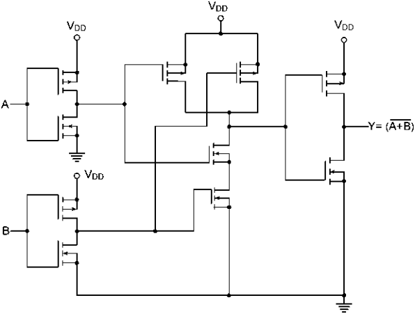
EXCLUSIVE-NOR Gate: An EXCLUSIVE-NOR gate is implemented using the logic diagram of Fig. 9(a).
As is evident from the figure, the output of this logic arrangement can be expressed by

Figure 9(b) shows the internal schematic of a two-input EX-NOR gate. MOSFETs Q1–Q4 constitute the NAND gate. MOSFETS Q5 and Q6 simulate ORing of A and B, and MOSFET Q7 provides ANDing of the NAND output with ORed output.
Since MOSFETs Q8–Q10 make up the complement of the arrangement of MOSFETs Q5–Q7, the final output is inverted. Thus, the schematic of Fig. 9(b) implements the logic arrangement of Fig. 9(a) and hence a two-input EX-NOR gate.
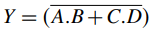
AND-OR-INVERT and OR-AND-INVERT Gates: Figure 10 shows the internal schematic of a typical two-wide, two-input AND-OR-INVERT gate. The output of this gate can be logically expressed by the Boolean equation
From the above expression, we can say that the output should be in a logic ‘0’ state for the following input conditions:
- When either AB = logic ‘1’ or CD = logic ‘1’
- When both AB and CD equal logic ‘1’.
For both these conditions there is a conduction path available from ground to output, which verifies that the circuit satisfies the logic expression. Also, according to the logic expression for the AND-ORINVERT gate, the output should be in a logic ‘1’ state when both AB and CD equal logic ‘0’. This implies that:
- Either A or B or both are in a logic ‘0’ state.
- Either C or D or both are in a logic ‘0’ state.
If these conditions are applied to the circuit of Fig. 10, we find that the ground will remain disconnected from the output and also that there is always a path from VDD to output. This leads to a logic ‘1’ at the output. Thus, we have proved that the given circuit implements the intended logic expression for the AND-OR-INVERT gate. The OR-AND-INVERT gate can also be implemented in the same way.
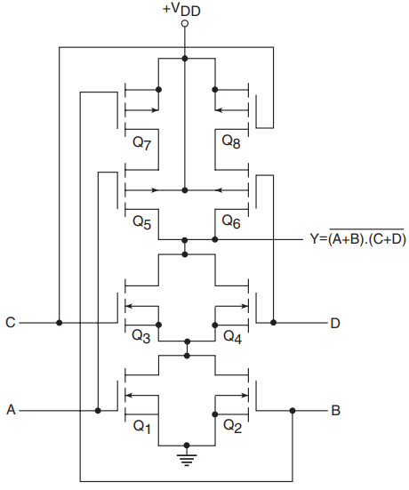
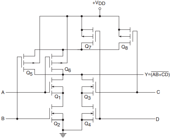
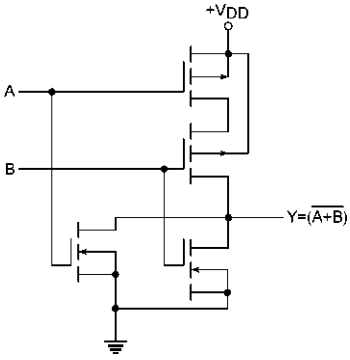
Figure 11 shows a typical internal schematic of a two-wide, two-input OR-AND-INVERT gate. The output of this gate can be expressed by the Boolean equation
It is very simple to draw the internal schematic of an AND-OR-INVERT or OR-AND-INVERT gate. The circuit has two parts, that is, the N-channel MOSFET part of the circuit and the P-channel part of the circuit.
Let us see, for instance, how the above Boolean equation relates to the circuit of Fig. 11. The fact that we need (A OR B) AND (C OR D) explains why the N-channel MOSFETs representing A and B inputs are in parallel and also why the N-channel MOSFETs representing C and D are also in parallel. The two parallel arrangements are then connected in series to achieve an ANDing operation. The complementary P-channel MOSFET section achieves inversion.
Note that the P-channel section is the complement of the N-channel section with N-channel MOSFETs replaced by P-channel MOSFETs and parallel connection replaced by series connection, and vice versa.
The operation of an AND-OR-INVERT gate can be explained on similar lines to the case of an OR-AND-INVERT gate. Expansion of both AND-OR-INVERT and OR-AND-INVERT gates should be obvious, ensuring that we do not have more than three devices in series.
Transmission Gate: The transmission gate, also called the bilateral switch, is exclusive to CMOS logic and does not have a counterpart in the TTL and ECL families. It is essentially a single-pole, single-throw (SPST) switch. The opening and closing operations can be controlled by externally applied logic levels. Figure 12(a) shows the circuit symbol.
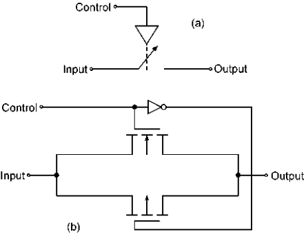
If a logic ‘0’ at the control input corresponds to an open switch, then a logic ‘1’ corresponds to a closed switch, and vice versa. The internal schematic of a transmission gate is nothing but a parallel connection of an N-channel MOSFET and a P-channel MOSFET with the control input applied to the gates, as shown in Fig. 12(b). Control inputs to the gate terminals of two MOSFETs are the complement of each other. This is ensured by an inbuilt inverter.
When the control input is HIGH (logic ‘1’), both devices are conducting and the switch is closed. When the control input is LOW (logic ‘0’), both devices are open and therefore the switch is open.
It may be mentioned here that there is no discrimination between input and output terminals. Either of the two can be treated as the input terminal for the purpose of applying input. This is made possible by the symmetry of the two MOSFETs.
It may also be mentioned here that the ON-resistance of a conducting MOSFET depends upon drain and source voltages. In the case of an N-channel MOSFET, if the source voltage is close to VDD, there is an increase in ON-resistance, leading to an increased voltage drop across the switch. A similar phenomenon is observed when the source voltage of a P-channel MOSFET is close to ground.
Such behaviour causes no problem in static CMOS logic gates, where source terminals of all N-channel MOSFETs are connected to ground and source terminals of all P-channel MOSFETs are connected to VDD.
This would cause a problem if a single N-channel or P-channel device were used as a switch. Such a problem is overcome with the use of parallel connection of N-channel and P-channel devices. Transmission gate devices are available in 4000-series as well as 74HC series of CMOS logic.
CMOS with Open Drain Outputs: The outputs of conventional CMOS gates should never be shorted together, as illustrated by the case of two inverters shorted at the output terminals (Fig. 13).
If the input conditions are such that the output of one inverter is HIGH and that of the other is LOW, the output circuit is then like a voltage divider network with two identical resistors equal to the ON-resistance of a conducting MOSFET. The output is then approximately equal to VDD/2, which lies in the indeterminate range and is therefore unacceptable. Also, an arrangement like this draws excessive current and could lead to device damage.
This problem does not exist in CMOS gates with open drain outputs. Such a device is the counterpart to gates with open collector outputs in the TTL family. The output stage of a CMOS gate with an open drain output is a single N-channel MOSFET with an open drain terminal, and there is no P-channel MOSFET. The open drain terminal needs to be connected to VDD through an external pull-up resistor.
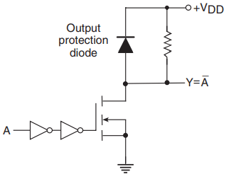
Figure 14 shows the internal schematic of a CMOS inverter with an open drain output. The pull-up resistor shown in the circuit is external to the device.
CMOS with Tristate Outputs: Like tristate TTL, CMOS devices are also available with tristate outputs. The operation of tristate CMOS devices is similar to that of tristate TTL. That is, when the device is enabled it performs its intended logic function, and when it is disabled its output goes to a high-impedance state. In the high-impedance state, both N-channel and P-channel MOSFETs are driven to an OFF-state.
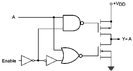
Figure 15 shows the internal schematic of a tristate buffer with active LOW ENABLE input. The circuit shown is that of one of the buffers in CMOS hex buffer type CD4503B. The outputs of tristate CMOS devices can be connected together in a bus arrangement, like tristate TTL devices with the same condition that only one device is enabled at a time.
Floating or Unused Inputs: Unused inputs of CMOS devices should never be left floating or unconnected. A floating input is highly susceptible to picking up noise and accumulating static charge. This can often lead to simultaneous conduction of P-channel and N-channel devices on the chip, which causes increased power dissipation and overheating.
Unused inputs of CMOS gates should either be connected to ground or VDD or shorted to another input. The same is applicable to the inputs of all those gates that are not in use.
For example, we may be using only two of the four gates available on an IC having four gates. The inputs of the remaining two gates should be tied to either ground or VDD.
Input Protection: Owing to the high input impedance of CMOS devices, they are highly susceptible to static charge build-up. As a result of this, voltage developed across the input terminals could become sufficiently high to cause dielectric breakdown of the gate oxide layer.
In order to protect the devices from this static charge build-up and its damaging consequences, the inputs of CMOS devices are protected by using a suitable resistor–diode network, as shown in Fig. 16(a).
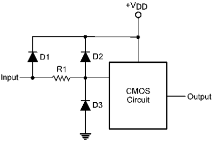
The protection circuit shown is typically used in metal-gate MOSFETs such as those used in 4000-series CMOS devices. Diode D2 limits the positive voltage surges to VDD + 0.7 V, while diode D3 clamps the negative voltage surges to −0.7 V.
Resistor R1 limits the static discharge current amplitude and thus prevents any damagingly large voltage from being directly applied to the input terminals. Diode D1 does not contribute to input protection. It is a distributed P–N junction present owing to the diffusion process used for fabrication of resistor R1.
The protection diodes remain reverse biased for the normal input voltage range of 0 to VDD, and therefore do not affect normal operation. Figure 16(b) shows a typical input protection circuit used for silicon-gate MOSFETs used in 74C, 74HC, etc., series CMOS devices. A distributed P–N junction is absent owing to R1 being a polysilicon resistor.
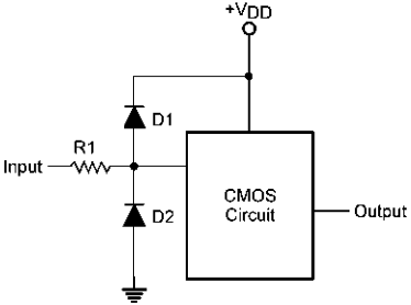
Diodes D1 and D2 do the same job as diodes D2 and D3 in the case of metal-gate devices. Diode D2 is usually fabricated in the form of a bipolar transistor with its collector and base terminals shorted.
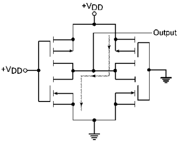
Latch-up Condition: This is an undesired condition that can occur in CMOS devices owing to the existence of parasitic bipolar transistors (NPN and PNP) embedded in the substrate. While N-channel MOSFETs lead to the presence of NPN transistors, P-channel MOSFETs are responsible for the existence of PNP transistors.
If we look into the arrangement of different semiconductor regions in the most basic CMOS building block, that is, the inverter, we will find that these parasitic NPN and PNP transistors find themselves interconnected in a back-to-back arrangement, with the collector of one transistor connected to the base of the other, and vice versa. Two such pairs of transistors connected in series exist between VDD and ground in the case of an inverter, as shown in Fig. 17.
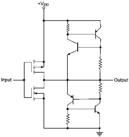
If for some reason these parasitic elements are triggered into conduction, on account of inherent positive feedback they get into a latch-up condition and remain in conduction permanently. This can lead to the flow of large current and subsequently to destruction of the device.
A latch-up condition can be triggered by high voltage spikes and ringing present at the device inputs and outputs. The device can also be prone to latch-up if its maximum ratings are exceeded.
Modern CMOS devices use improved fabrication techniques so as to minimize factors that can cause this undesired effect. The use of external clamping diodes at inputs and outputs, proper termination of unused inputs and regulated power supply with a current-limiting feature also helps in minimizing the chances of occurrence of the latch-up condition and in minimizing its effects if it occurs.
Subfamilies of CMOS Logic Family
In the following paragraphs, we will briefly describe various subfamilies of CMOS logic, including subfamilies of the 4000 series and those of TTL pin-compatible 74C series.
4000-series: The 4000A-series CMOS ICs, introduced by RCA, were the first to arrive on the scene from the CMOS logic family. The 4000A CMOS subfamily is obsolete now and has been replaced by 4000B and 4000UB subfamilies. We will therefore not discuss it in detail.
The 4000B series is a high-voltage version of the 4000A series, and also all the outputs in this series are buffered. The 4000UB series is also a high-voltage version of the 4000A series, but here the outputs are not buffered.
A buffered CMOS device is one that has constant output impedance irrespective of the logic status of the inputs. If we recall the internal schematics of the basic CMOS logic gates, we will see that, with the exception of the inverter, the output impedance of other gates depends upon the logic status of the inputs. This variation in output impedance occurs owing to the varying combination of MOSFETs that conduct for a given input combination.
All buffered devices are designated by the suffix ‘B’ and referred to as the 4000B series. The 4000-series devices that meet 4000B series specifications except for the VIL and VIH specifications and that the outputs are not buffered are called unbuffered devices and are said to belong to the 4000UB series.
Figures 18 and 19 show a comparison between the internal schematics of a buffered two-input NOR (Fig. 18) and an unbuffered two-input NOR (Fig. 19).
A buffered gate has been implemented by using inverters at the inputs to a two-input NAND whose output feeds another inverter. This is the typical arrangement followed by various manufacturers, as the inverters at the input enhance noise immunity.
Another possible arrangement would be a two-input NOR whose output feeds two series-connected inverters. Variation in the output impedance of unbuffered gates is larger for gates with a larger number of inputs.
For example, unbuffered gates have an output impedance of 200–400Ω in the case of two-input gates, 133–400Ω for three-input gates and 100–400Ω for gates with four inputs. Buffered gates have an output impedance of 400Ω . Since they have the same maximum output impedance, their minimum IOL and IOH specifications are the same.
Characteristic features of 4000B and 4000UB CMOS devices are as follows:
- VIH (buffered devices) = 3.5 V (for VDD = 5 V), 7.0 V (for VDD= 10 V) and 11.0 V (for VDD = 15 V);
- VIH (unbuffered devices) = 4.0 V (for VDD= 5 V), 8.0 V (for VDD = 10 V) and 12.5 V (for VDD = 15 V);
- IIH = 1.0 µA; IIL = 1.0 µA;
- IOH = 0.2 mA (for VDD = 5 V), 0.5 mA (for VDD = 10 V) and 1.4 mA (for VDD = 15 V);
- IOL = 0.52 mA (for VDD = 5 V), 1.3 mA (for VDD= 10 V) and 3.6 mA (for VDD = 15 V);
- VIL (buffered devices) = 1.5 V (for VDD = 5 V), 3.0 V (for VDD= 10 V) and 4.0 V (for VDD= 15 V);
- VIL (unbuffered devices) = 1.0 V (for VDD = 5 V), 2.0 V (for VDD= 10 V) and 2.5 V (for VDD = 15 V);
- VOH = 4.95 V (for VDD = 5 V), 9.95 V (for VDD =10 V) and 14.95 V (for VDD = 15 V);
- VOL = 0.05 V; VDD = 3 – 15 V;
- propagation delay (buffered devices) = 150 ns (for VDD = 5 V), 65 ns (for VDD = 10 V) and 50 ns (for VDD = 15 V);
- propagation delay (unbuffered devices) = 60 ns (for VDD = 5 V), 30 ns (for VDD = 10 V) and 25 ns (for VDD = 15 V);
- noise margin (buffered devices) = 1.0 V (for VDD = 5 V), 2.0 V (for VDD = 10 V) and 2.5 V (for VDD= 15 V);
- noise margin (unbuffered devices) = 0.5 V (for VDD = 5 V), 1.0 V (for VDD = 10 V) and 1.5 V (for VDD= 15 V);
- output transition time (for VDD = 5 V and CL = 50 pF) = 100 ns (buffered devices) and 50–100 ns (for unbuffered devices);
- power dissipation per gate (for f = 100 kHz) = 0.1 mW;
- speed–power product (for f = 100 kHz) = 5 pJ;
- maximum flip-flop toggle rate = 12 MHz.
74C Series: The 74C CMOS subfamily offers pin-to-pin replacement of the 74-series TTL logic functions. For instance, if 7400 is a quad two-input NAND in standard TTL, then 74C00 is a quad two-input NAND with the same pin connections in CMOS. The characteristic parameters of the 74C series CMOS are more or less the same as those of 4000-series devices.
74HC/HCT Series: The 74HC/HCT series is the high-speed CMOS version of the 74C series logic functions. This is achieved using silicon-gate CMOS technology rather than the metal-gate CMOS technology used in earlier 4000-series CMOS subfamilies. The 74HCT series is only a process variation of the 74HC series.
The 74HC/HCT series devices have an order of magnitude higher switching speed and also a much higher output drive capability than the 74C series devices. This series also offers pin-to-pin replacement of 74-series TTL logic functions. In addition, the 74HCT series devices have TTL-compatible inputs.
74AC/ACT Series: The 74AC series is presently the fastest CMOS logic family. This logic family has the best combination of high speed, low power consumption and high output drive capability. Again, 74ACT is only a process variation of 74AC. In addition, 74ACT series devices have TTL-compatible inputs. The characteristic parameters of the 74C/74HC/74HCT/74AC/74ACT series CMOS are summarized as follows (for VDD= 5 V):
- VIH (min.) = 3.5 V (74C), 3.5 V (74HC and 74AC) and 2.0 V (74HCT and 74ACT);
- VOH (min.) = 4.5 V (74C) and 4.9 V (74HC, 74HCT, 74AC and 74ACT);
- VIL(max.) = 1.5 V (74C), 1.0 V (74HC), 0.8 V (74HCT), 1.5 V (74AC) and 0.8 V (74ACT);
- VOL (max.) = 0.5 V (74C) and 0.1 V (74HC, 74HCT, 74AC and 74ACT);
- IIH(max.) = 1µA; IIL (max.) = 1 µA;
- IOH (max.) = 0.4 mA (74C), 4.0 mA (74HC and 74HCT) and 24 mA (74AC and 74ACT);
- IOL (max.) = 0.4 mA (74C), 4.0 mA (74HC and 74HCT) and 24 mA (74AC and 74ACT);
- VNH = 1.4 V (74C, 74HC and 74AC) and 2.9 V (74HCT and 74ACT);
- VNL = 1.4 V (74C), 0.9 V (74HC), 0.7 V (74HCT and 74ACT) and 1.4 V (74AC);
- propagation delay = 50 ns (74C), 8 ns (74HC and 74HCT) and 4.7 ns (74AC and 74ACT);
- power dissipation per gate (for f = 100 kHz) = 0.1 mW (74C), 0.17 mW (74HC and 74HCT) and 0.08 mW (74AC and 74ACT);
- speed–power product (for f = 100 kHz) = 5 pJ (74C), 1.4 pJ (74HC and 74HCT) and 0.37 pJ (74AC and 74ACT);
- maximum flip-flop toggle rate = 12 MHz (74C), 40 MHz (74HC and 74HCT) and 100 MHz (74AC and 74ACT).
Related Posts
- Logic Gates
- Significance & Types of Logic Family
- Characteristics Parameters of Logic Families
- TTL Logic Family
- ECL Logic Family
- CMOS Logic Family
- Interfacing of Logic Families
- Microcontroller Architecture
- Components of Microcontroller
- Interfacing Devices with Microcontroller
- IC Based Multivibrator Circuits
- Astable, Monostable & Bistable Multivibrator
- Logic Analyser
- Types of Oscilloscope
- Frequency Synthesizers
- Frequency Counter