Thyristors are a family of semiconductor switches having four or more layers, that is, p-n-p-n type of structure. Nowadays, thyrsitors with blocking voltage in excess of 6 kV and continuous current rating in excess of 4 kA are available.
In a thyristor, if the ohmic connection is made to the first p-region and the last n-region and no other connection is made in the intermediate region, then the device is called a diode thyristor.
If an additional connection is made to the intermediate n- or p-region, the device is called triode thyristor and if the connection is made to both the intermediate regions, the device is called terode thyristor.
The simplest in structure and most common thyristor is reverse blocking triode thyristor, also called as the siliconcontrolled rectifier (SCR) and the more complex thyristor structure is the bi-directional triode thyristor or TRIAC.
A large number of other devices similar to basic thyristors have also been developed. These include, inverter grade fast thyristors, diac, triac, the gate turn-off thyristors (GTO), silicon controlled switch (SCS), light activated SCR (LASCR), asymmetrical thyristor (ASCR) and reverse conducting thyristor (RCT).
From the construction and operational perspective, a thyristor is a four layer, three terminal minority carrier semi-controlled device. It can be turned on by a current signal but cannot be turned off without interrupting the main current.
The major advantage of thyristor is that it can block voltage in both directions but can conduct current only in one direction. It offers very low forward voltage drop during conduction even with a large current.
One of the main drawbacks is that the thyristors have longer switching times (tens of μs) in comparison to BJTs and most of the other switching devices.
The other drawback associated with its use as a switching device is that it cannot be turned off only by withdrawal of the control input.
As a result these are not used in high frequency switching appliances but continue to be used in power frequency AC applications in which the current naturally goes through zero, due to their low conduction loss, requirement of low control power and reverse voltage blocking capability. Thyristors are a popular choice for use in very high power applications (excess of 50 MW) like for AC-DC phase controlled converters and AC-AC cyclo-converters.
Operation of Thyristors
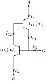
Figures 1(a) and (b) show the circuit symbol and typical constructional details of a thyristor, respectively.
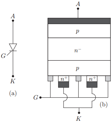
(b) Constructional features.
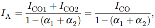
The basic operating principle of a thyristor, can be best understood by two transistor analogy or modeling it as two BJTs connected as shown in Fig. 2. The equivalent circuit of a thyristor can be considered to be constituted by two transistors (p-n-p-n device) as shown.
With the gate open or shorted to the cathode, the device is considered OFF and no current flows from anode to cathode, apart from low leakage current.
In the p-n-p-n device with forward voltage applied, (anode is positive with respect to the cathode), the gate terminal is open, the junctions J1 and J3 are forward biased, and J2 is reverse biased.
Under this condition, the collector current IC1 of transistor Q1 and IC2 of transistor Q2 are given by,
IC1 = α1IA + ICO1
IC2 = α2IK + ICO2 ……..(equation 1)
Where α1 and α2 are current gains of Q1 and Q2, respectively, and ICO1 and ICO2 are reverse saturation currents of the CB junctions of Q1 and Q2, respectively.
Now from the two transistor equivalent circuit shown in of Fig. 2, we have
IC1 + IC2 = IA ……..(equation 2)
IA = IK ( ∵ IG = 0 ) ……..(equation 3)
Combining Eqs. (2) and (3), we get
Where ICO = ICO1 + ICO2 is the total reverse leakage current of J2 junction.
When the anode to cathode voltage VAK is small, ICO is very low and both α1 and α2 are much lower than unity. Therefore, total anode current IA, as given in Eq. (4) is very near to ICO.
But when VAK is increased up to the avalanche breakdown voltage of the junction J2, ICO begins to increase at a fast rate due to avalanche multiplication process.
Consequently both α1 and α1 increase and (α1 + α1) approaches near unity in Eq. (4). Therefore, the anode current IA will increase and can be restricted only by the external load resistance.
However, as the applied voltage is the same and the voltage drop in the external resistance increases due to higher anode current, a collapse of voltage across the thyristor occurs. Thus the CB junctions of both Q1 and Q2 become forward biased and the total voltage drop across the device becomes somewhat greater than a diode drop.
Under this condition, the thyristor is said to be in ON state. Just after turning ON, if IA is kept at a larger value than a specified threshold current called the latching current IL, α1 and α2 remain high enough to keep the thyristor in ON state. The gate loses complete control of the device and it cannot be turned OFF through the gate.
The thyristor can be turned OFF only if the anode current IA is brought below another specified current called the holding current (IH) where the current gains α1 and α2 get reduced to a very low value.
The thyristor can regain forward blocking capacity once excess stored charges at the junction J2 are removed by application of a reverse voltage across anode A and cathode K.
Alternately, thyrsitor can be turned ON if an external positive current pulse is applied to the gate at lower forward voltages across the device below the forward break-over level.
With a positive gate current applied between the gate and cathode terminals, Eq. (3) can be modified as,
IK = IA + IG ……..(equation 5)
Combining Eqs. (4) and (5), we get
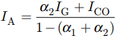
It can be observed from Eq. (6) that with large value of IG, the thyristor can be turned ON for lower value of ICO or VAK.
This method is known as gate assisted turn-on of a thyristor and is the commonly used method with which a thyristor is turned ON.
With application of reverse voltage across a thyristor (i.e., making cathode positive with respect to anode, the junctions J1 and J3 get reverse biased, while J2 is forward biased.
The junction J3 has lower reverse breakdown voltage compared to the other junctions as both the n+ and p– regions on either side of this junction are heavily doped. Therefore, the reverse voltage almost completely comes across junction J1.
The maximum value of the reverse voltage that can be applied is restricted by the following factors:
- The maximum tolerable field strength at junction J1 at which its avalanche breakdown occurs.
- The punch through capacity of the lightly doped n− layer.
The maximum reverse that can be applied across a thyristor is generally expressed by the term peak inverse voltage (PIV) also called reverse break over voltage (VBR).
Related Posts
- Operation of Thyristors
- Static Characteristics of SCR | Thyristor
- Silicon Controlled Rectifier Function
- Applications & Characteristics of SCR
- SCR Selection Criteria
- Thyristor | SCR Specifications and Ratings
- Operation of Triac & GTO
- Triac Working
- Characteristics, Operation, & Construction of IGBT
- Freewheeling Diode in Controlled Rectifier
- Reverse Recovery Characteristics of Power Diode