Static Characteristics of SCR
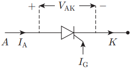
Figure 1(a) shows the circuit symbol and the conventions for the different variables used in the V-I characteristics of the thyristor, shown in Fig. 1(b).
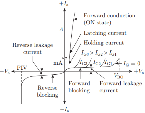
The different modes describing the V-I characteristics are as follows:
1. Forward blocking mode: In Fig. 1(b), in forward blocking mode, when gate current IG = 0, the applied anode-cathode voltage VAK has to increase up to forward break over voltage VBO to start the conduction of thyristor.
2. Forward conduction mode: In this mode, the forward break over takes place at VBO and the voltage across the thyristor drops to a small voltage VH or the holding voltage which is slightly above the diode conduction drop.
Beyond this point, voltage across the thyristor is assumed to remain constant at VH which is generally 1.15 V, while the anode current is determined by the external load. The magnitude of gate current has a very strong effect on the value of the forward break over voltage VBO as shown in the Fig. 1(b).
It is observed that the forward break over voltage (VBO) reduces drastically with increase of the gate current (IG).
After turning ON, the thyristor is no longer affected by the gate current. Hence, any current pulse of required magnitude which is longer than the minimum duration needed for `turning ON’ is sufficient to drive the thyristor into conduction.
This minimum gate pulse width or duration is basically decided by the external circuit to allow the device current to rise above its latching current (IL) level.
3. Forward blocking mode: This mode is described in the third quadrant of the characteristics in Fig. 1(b), which is the reverse V-I characteristics of the thyristor.
Once the thyristor is ON, the only way to turn it OFF is by bringing the thyristor current below holding current (IH), as has been described earlier. The gate terminal has no control over the turn-OFF process of the thyristor.
For the AC circuits with resistive load the turn-OFF process happens automatically during negative zero crossing of the supply voltage as the current also follows the same path to go to negative value (less than IH) and thereby turning of the device. This turn-OFF phenomenon is called natural commutation or line commutation.
However, in DC circuits, due to the absence of the negative zero crossings, some additional circuit arrangement has to be made to ensure this condition. This process of turning OFF the device is called forced commutation.
During the reverse blocking stage, that is, in quadrant three of the characteristics, if IG = 0 then only reverse saturation current (IS) flows through the thyristor until the reverse voltage reaches peak inverse voltage or PIV (also called reverse breakdown voltage (VBR) of the device).
At this point, the current starts to rise sharply and this large reverse voltage current generates excessive heat and destroys the device. If the gate current is not removed or IG > 0 during reverse bias condition, it give rise to the reverse saturation current.
Thyristor Turn-ON Methods
The various turn-ON methods for thyristors are described as follows.
1. Gate triggering: This has been already described under the thyristor characteristics. Like the BJTs, the thyristor are also current operated devices. Thus, the gate current of proper amplitude is to be provided at the gate terminal by providing a voltage between gate to cathode for proper turn-ON of the device.
The typical arrangement is shown in Fig. 2. The typical gate to cathode voltage varies between 5—10 V and typical gate current can be between 10 to 500 mA or it may even reach 1 A. The increased values of current are required for thyristor of higher current ratings.
As has been mentioned under thyristor characteristics, the gate current has no role after the device has turned ON. Usually the gate current is provided in pulsed mode. The pulse width is so adjusted that it is sufficient for the thyristor current to reach the latching current value during the presence of the pulse.
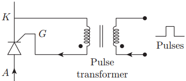
The gate triggering circuit also needs isolation from the power circuit, which is provided through a pulse transform. The frequency of the pulse trains provided at the gate is high and therefore to reduce eddy losses in the core, ferrites are used in the pulse transformers. This technique is widely used to trigger the thyristors.
2. Forward voltage triggering: In this method, when the forward voltage between anode to cathode is increased over the forward break over voltage VBO with gate circuit open, the thyristor triggers.
This technique can be used for lower VBO rating of thyristor below 100 V, but is seldom used for the thyristor with VBO higher, than 200 V.
3. Temperature triggering: In this method, the forward blocking condition of the thyristor is utilized where heat developed by the leakage current through junction J2 in this condition is utilized.
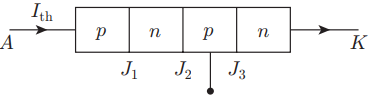
This can cause vanishing of the depletion layer of the reverse biased junction J2 and make the device turn ON. The junction arrangement of the device is shown in Fig. 3. In this mode of turn-ON, the gate circuit is always open.
4. dv/dt Triggering: Sometimes, high dv/dt appearing across the junction J2 can lead to the vanishing of its depletion layer and cause turn-ON. This is simply because
ij2 = edvj2 ÷ dt
If dv/dt is high, the current of this junction can be high to turn on the thyristor. This method is seldom used and rather this phenomenon can cause spurious turn-ON of the thyristor which is to be prevented through appropriate snubber circuits.
Thyristor Protection Methods
The various methods of thyristor protection are listed as follows:
1. di/dt Protection: When the thyristor is switched on, its current rises and reaches the final value decided by the load connected to it. But the rate of rise of the current, which is also decided by the inductive nature of the load, can cause damage of the thyristor junction J2 if exceeded above a certain value.
The high di/dt can cause hot spots in the junction J2 which injects more current though that area due to negative temperature co-efficient nature of the junction. Thus the current further increases and causes the damage spot to spread and the entire junction breaks down. Thus proper projection to limit the impressed di/dt under the allowable value has to be provided. This is achieved connecting an inductor (L) is series with the device to form a snubber circuit.
2. dv/dt Protection: When the forward voltage is impressed on the thyristor and if the dv/dt is more than the allowable dv rating, the thyristor can undergo spurious turn ON. The dv/dt in reverse direction is also developed during turn-ON situation. The high dv/dt can even damage the thyristor junctions.
Thus, a circuit, usually consisting of R and C in series combination is connected in parallel with the thyristor, is used to protect it from high dv/dt being impressed upon it when subjected to any voltage stress during turn-OFF or turn-ON process.
The combination of R, L and C connected to the thyristors for protection purpose is called snubber circuit. The inductor L limits the di/dt for the device and capacitor C limits the dv/dt stress on the device. The connection of an inductor L, resistor R and capacitor C in a snubber circuit is depicted in Fig. 4.
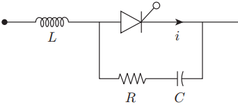
protection.
The inductance L is usually calculated from the thyristor safe di/dtmax rating and maximum voltage that can be applied across it as,
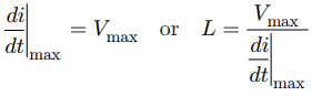
The R and C for the snubber circuit can be calculated from the following empirical relationships:
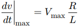
Where dv/dtmax is the maximum allowable dv/dt rating for the device and
R = 2D√(L/C) (Equation 3)
The factor D is known as damping factor and usually taken as 0.5. Thus substituting for from Eq. (3) in Eq. (2), we get,
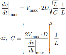
The value of C can be substituted in Eq. (3) to find R.
Related Posts
- Operation of Thyristors
- Static Characteristics of SCR | Thyristor
- Silicon Controlled Rectifier Function
- Applications & Characteristics of SCR
- SCR Selection Criteria
- Thyristor | SCR Specifications and Ratings
- Operation of Triac & GTO
- Triac Working
- Characteristics, Operation, & Construction of IGBT
- Freewheeling Diode in Controlled Rectifier
- Reverse Recovery Characteristics of Power Diode