TRIAC (Triode thyristor for alternating current) or triac is a bi-directional thyristor switch mainly used for AC control applications.
It conducts in both directions, unlike the thyristors (SRCs) which conduct in one direction only. It can be considered to be equivalent to two thyristors connected in anti-parallel but having only three terminals.
It has a gate terminal that is used for controlling the turn-ON of triac and as in thyristors, the conduction is initiated by injecting a current pulse into the gate terminal.
The gate loses control over conduction once the triac is turned on in a similar manner to a thyristor. The triac turns off only when the current through the main terminals become zero or less than the holding current level.
Operation of Triac
Figures 1(a) and (b) show the circuit symbol and schematic representation of a Triac when it is conducting in both the directions.
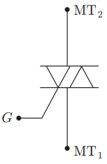
As the triac is bi-directional, that is, can conduct in both the directions, its terminals are called main terminal 1 and 2 (MT1 and MT2) and the gate is denoted by G.
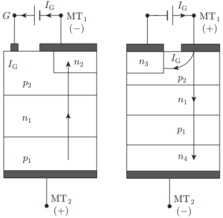
Figure 1(b), shows that the gate terminal is near MT1 and is connected to both n3 and p2 regions by metallic contact during the conduction in both directions.
Similarly MT1 is connected to n2 and p2 regions while MT2 is connected to n4 and p1 regions for conduction in both directions.
There are different ways in which the gate can be fired and the most common is with reference to MT1.
The direction of current flow is decided by the polarity of voltage across MT1 and MT2 and the gate pulse is always positive irrespective of direction of current flow.
In the trigger mode-1 [Fig. 1(b)] for conduction of current from MT1 to MT2, the gate pulse is applied between gate and MT1 terminal. In this mode the gate current flows mainly through the p2n2 junction as in a normal thyristor.
When the gate current is sufficient such that adequate amount of charges have been injected into p2 layer, the triac starts conducting through the p1n1p2n2 layers as in a regular thyristor.
In the trigger mode-2 [Fig. 1(c)], for conduction of current from MT1 to MT2, the negative gate current IG forward biases the p2n3 junction and a large number of electrons are injected in the p2 region by n3 and the structure p2n1p1n4 turns ON fully.
Static Characteristics of Triac
The static or steady state V-I characteristics of triac is depicted in Fig. 2.
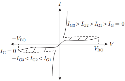
When no signal applied to the gate, the triac blocks both the half cycles of the applied AC voltage provided its peak value is lower than the break over voltage (VBO) of the device.
However, the turning ON of the triac can be controlled in either direction by applying the gate trigger pulse of appropriate current at the desired instance.
Trigger mode-1 is used in the first quadrant where the current flows from MT2 to MT1 and trigger mode-2 is used in the third quadrant where the current flows from MT1 to MT2.
Most of the thyristor characteristics parameters such as latching and holding current are also applicable to the triac. However, as the triac has two conducting paths from MT1 to MT2 and from MT2 to MT1, their interaction lead to the complex structure of the triac.
Gate Turn-Off Thyristor (GTO)
We have seen that a thyristor (SRC) cannot be turned-OFF by gate control and requires an additional turn-OFF or commutation circuit. A gate turn-OFF (GTO) thyristor is a current controlled bipolar type of device that provided turn-OFF through gate terminal. Thus its main difference from a thyristor lies in its commutation procedure.
The GTOs are designed to turn-OFF when a negative current is sent through the gate, which causes reversal of the gate current. During conduction, the device behaves just like a thyristor with very low ON state voltage drop. The most popular variety of GTO has no substantial reverse voltage blocking capabilities.
Construction of GTO
The circuit symbol and schematic representation of a GTO is shown in Figs. 3(a) and (b), respectively. The two-way arrow convention on the gate lead distinguishes the GTO from the regular thyristor.
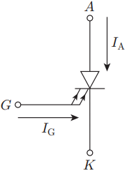
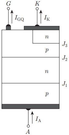
A GTO has a four layer p-n-p-n semiconductor switching device with three p-n junctions similar to a thyristor as it can be turned ON by a positive gate current pulse and can be turned OFF by a negative gate pulse.
The cathode n+ layer is heavily doped to obtain high emitter efficiency. The doping level of the p– type gate region graded to provide good emitter efficiencies. Good emitter efficiency needs the doping level to be low, while to provide good turn-OFF characteristics needs high doping level.
Operation of GTO
Since the GTO is similar in structure to thyristor with a four-layer p-n-p-n structure the basic operating principle can be explained similarly using the two transistor (BJT) model.
The GTO can be represented by the two transistor equivalent structure as shown in Fig. 4.
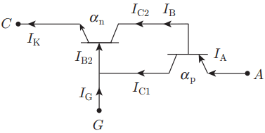
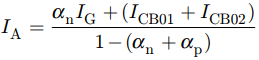
In the circuit, the collector and base current are given
IC1 = αpIA + ICB01 (Equation 1)
IK = IA + IG and IA = IB1 + IC1 (Equation 2)
Combining Eqs. (1) and (2), we get
To turn-OFF a conducting GTO, the gate terminal is biased negative with respect to the cathode and removal of excess charge from the gate is an important part of turn-OFF process. The amount of current to be withdrawn from gate is about one third to one fourth of the conducting anode current. This is reason the device is known as gate turn-OFF thyristor or GTO.
Related Posts
- Operation of Thyristors
- Static Characteristics of SCR | Thyristor
- Silicon Controlled Rectifier Function
- Applications & Characteristics of SCR
- SCR Selection Criteria
- Thyristor | SCR Specifications and Ratings
- Operation of Triac & GTO
- Triac Working
- Characteristics, Operation, & Construction of IGBT
- Freewheeling Diode in Controlled Rectifier
- Reverse Recovery Characteristics of Power Diode