Analog to Digital Conversion
Physical quantities like temperature, pressure, velocity etc. can be measured using transducer circuits. The resulting analog voltage produced by a transducer is often converted to digital form so that it can be processed by a computer or a digital signal processor (DSP). The conversion of an analog signal to digital utilizes a sample-and- hold circuit, which is covered in this section, followed by an analog-to-digital converter (ADC), which is discussed in the next section.
Sample-and-Hold Circuit
A sample-and-hold circuit samples an analog input voltage at a certain point in time and retains or holds the sampled voltage for an extended time after the sample is taken. The sample-and-hold process keeps the sampled analog voltage constant for the length of time necessary to allow an analog-to-digital converter (ADC) to convert the voltage to digital form.

A basic sample-and-hold circuit consists of an analog switch, a capacitor, and input and output amplifiers as shown in Figure 1. The analog switch samples the analog input voltage through the input amplifier, the capacitor (CH) stores or holds the sampled voltage for a period of time, and the output amplifier provides a high input impedance to prevent the capacitor from discharging quickly.

As illustrated in Figure 2, a relatively narrow control voltage pulse closes the analog switch and allows the capacitor to charge to the value of the input voltage. The switch then opens, and the capacitor holds the voltage for a long period of time because of the very high impedance discharge path through the op-amp input.

A more detailed sample-and-hold circuit is shown in Figure 3. The analog switch is implemented with a JFET.
Perhaps a more appropriate name for the sample-and-hold process is sample/track-and- hold because the circuit actually tracks the input voltage during the sample interval.


As indicated in Figure 4, the output follows the input during the time that the control voltage is high; and when the control voltage goes low, the last voltage is held until the next sample interval.
Performance Specifications of Sample-and-Hold Circuits
Several specifications apply to sample-and-hold circuits. These include the aperture time, aperture jitter, acquisition time, droop, and feedthrough. Each of these parameters is illustrated in Figure 5 for an example input voltage waveform.

- Aperture time: the time for the analog switch to fully open after the control voltage switches from its sample level to its hold level. Aperture time produces a delay in the effective sample point.
- Aperture jitter: the uncertainty in the aperture time.
- Acquisition time: the time required for the device to reach its final value when the control voltage switches from its hold level to its sample level.
- Droop: the change in voltage from the sampled value during the hold interval because of charge leaking off of the hold capacitor.
- Feedthrough: the component of the output voltage that follows the input signal after the analog switch is opened. The inherent capacitance from the input to the output of the switch causes feedthrough.
Analog to Digital Conversion
Analog-to-digital conversion is the process of converting the output of the sample-and-hold circuit to a series of binary codes that represent the amplitude of the analog input at each of the sample times. The sample-and-hold process keeps the amplitude of the analog input signal constant between sample pulses; therefore, the analog-to-digital conversion can be done using a constant value rather than having the analog signal change during a conversion interval, which is the time between sample pulses.
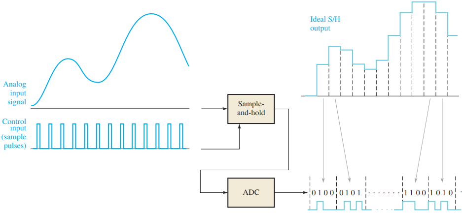
Figure 6 illustrates the basic function of an ADC (analog-to-digital converter). The sample intervals are indicated by dashed lines. The tracking intervals are not shown on the S/H output because they are assumed to be very short and can be neglected.
Conversion Parameters
Resolution: An analog-to-digital converter (ADC) translates a continuous analog signal into a series of binary numbers. Each binary number represents the value of the analog signal at the time of conversion. The resolution of an ADC can be expressed as the number of bits (binary digits) used to represent each value of the analog signal.
A 4-bit ADC can represent sixteen different values of an analog signal because 24 = 16. An 8-bit ADC can represent 256 different values of an analog signal because 28 = 256. A 12-bit ADC can represent 4096 different values of the analog signal because 216 = 4096.
The more bits, the more accurate is the conversion and the greater is the resolution because more values of a given analog signal can be represented.
Conversion Time: In addition to resolution, another important characteristic of ADCs is conversion time. The conversion of an analog voltage into a digital quantity is not an instantaneous event, but it is a process that takes a certain amount of time. The conversion time can range from microseconds for fast converters to milliseconds for slower devices.

Conversion time is illustrated in a basic way in Figure 7. As you can see, the analog voltage (v0) to be converted occurs at time t0 but the conversion is not complete until time t1.
Quantization Error: The term quantization in this context refers to determining a value for a changing analog voltage. Ideally, we would like to assign a number to the voltage at a given instant and convert it immediately to digital form. This is, of course, impossible because of the conversion time of ADCs.
Since an analog signal may change during a conversion time, the voltage at the end of the conversion time may not be the same as it was at the beginning. This change in voltage during the conversion time Δv, produces what is called the quantization error, as illustrated in Figure 8.

One way to avoid or at least minimize quantization error is to use a sample-and-hold circuit at the input to the ADC. The sample-and-hold circuit quickly samples the analog input and then holds the sampled voltage for a certain time.
When used in conjunction with an ADC, the sample-and-hold is held constant for the duration of the conversion time. This allows the ADC to convert a constant voltage to digital form and avoids the quantization error.

A basic illustration of this process is shown in Figure 8. When compared to the conversion in Figure 7, you can see that a more accurate value of the analog input at the desired sample point is achieved.
Sampling: In A/D conversion, an analog waveform is sampled at a given point and the sampled value is then converted to a binary number. Since it takes a certain interval of time to accomplish the conversion, the number of samples of an analog waveform during a given period of time is limited.
For example, if a certain ADC can make one conversion in 1 ms, it can make 1000 conversions in one second. That is, it can convert 1000 different analog values to digital form in a one-second interval.
In order to represent an analog waveform, the sample rate must be greater than twice the maximum frequency component of the analog signal. The theoretical minimum limit of the sampling rate is known as the Nyquist rate or frequency. At the Nyquist rate, an analog signal is sampled and converted two times per cycle.


In practice, however, a signal must be sampled more than twice per cycle. Obviously, a greater number of samples per cycle of the analog signal results in a more accurate representation of the analog signal. This is illustrated in Figure 9 for two different sample rates. The light blue waveforms are the sample-and-hold outputs for two sample rates. As you can see, the higher rate produces a more accurate result.
Flash Method of Analog-to-Digital Conversion
Several methods can be used in analog-to-digital conversion, and we will briefly look at one called the simultaneous or flash method. Another commonly used method is known as successive approximation.
The flash method uses several comparators to compare reference voltages with the analog input from a sample-and-hold circuit. When the analog voltage exceeds the reference level for a given comparator, a high-level output is produced by the comparator.

Figure 10 shows a simplified flash ADC that uses seven comparators for a conversion to three binary bits. The comparator outputs go to a priority encoder, which is a digital circuit that produces a binary output code that represents the level of the input. A 4-bit ADC of this type requires fifteen comparators. In general, 2n – 1 comparators are required for conversion to an n-bit binary code.
The large number of comparators necessary for a practical size binary code is one disadvantage of the flash method. Its chief advantage is that it provides a fast conversion time. The resistive voltage-divider sets the reference voltage for each comparator.
The output of each comparator is connected to an input of the priority encoder. A start-conversion pulse for each sampled level enables the encoder, and an encoder produces a 3-bit code representing the value of the sampled analog level.