Characteristics Parameters of Logic Families
In this atricle, we will briefly describe the parameters used to characterize different logic families. Some of these characteristic parameters, as we will see in the paragraphs to follow, are also used to compare different logic families.
HIGH-level input current, IIH. This is the current flowing into (taken as positive) or out of (taken as negative) an input when a HIGH-level input voltage equal to the minimum HIGH-level output voltage specified for the family is applied.
In the case of bipolar logic families such as TTL, the circuit design is such that this current flows into the input pin and is therefore specified as positive. In the case of CMOS logic families, it could be either positive or negative, and only an absolute value is specified in this case.
LOW-level input current, IIL. The LOW-level input current is the maximum current flowing into (taken as positive) or out of (taken as negative) the input of a logic function when the voltage applied at the input equals the maximum LOW-level output voltage specified for the family.
In the case of bipolar logic families such as TTL, the circuit design is such that this current flows out of the input pin and is therefore specified as negative. In the case of CMOS logic families, it could be either positive or negative. In this case, only an absolute value is specified.
HIGH-level and LOW-level input current or loading are also sometimes defined in terms of unit load (UL). For devices of the TTL family, 1 UL (HIGH) = 40 µA and 1 UL (LOW) = 1.6 mA.
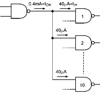
HIGH-level output current, IOH. This is the maximum current flowing out of an output when the input conditions are such that the output is in the logic HIGH state. It is normally shown as a negative number. It tells about the current sourcing capability of the output. The magnitude of IOH determines the number of inputs the logic function can drive when its output is in the logic HIGH state.
For example, for the standard TTL family, the minimum guaranteed IOH is −400µ A, which can drive 10 standard TTL inputs with each requiring 40µ A in the HIGH state, as shown in Fig. 1.
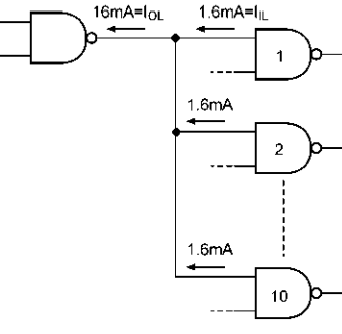
LOW-level output current, IOL. This is the maximum current flowing into the output pin of a logic function when the input conditions are such that the output is in the logic LOW state. It tells about the current sinking capability of the output. The magnitude of IOL determines the number of inputs the logic function can drive when its output is in the logic LOW state.
For example, for the standard TTL family, the minimum guaranteed IOL is 16 mA, which can drive 10 standard TTL inputs with each requiring 1.6 mA in the LOW state, as shown in Fig. 2.
HIGH-level off-state (high-impedance state) output current, IOZH. This is the current flowing into an output of a tristate logic function with the ENABLE input chosen so as to establish a high-impedance state and a logic HIGH voltage level applied at the output. The input conditions are chosen so as to produce logic LOW if the device is enabled.
LOW-level off-state (high-impedance state) output current, IOZL. This is the current flowing into an output of a tristate logic function with the ENABLE input chosen so as to establish a high-impedance state and a logic LOW voltage level applied at the output. The input conditions are chosen so as to produce logic HIGH if the device is enabled.
HIGH-level input voltage, VIH. This is the minimum voltage level that needs to be applied at the input to be recognized as a legal HIGH level for the specified family. For the standard TTL family, a 2 V input voltage is a legal HIGH logic state.
LOW-level input voltage, VIL. This is the maximum voltage level applied at the input that is recognized as a legal LOW level for the specified family. For the standard TTL family, an input voltage of 0.8 V is a legal LOW logic state.
HIGH-level output voltage, VOH. This is the minimum voltage on the output pin of a logic function when the input conditions establish logic HIGH at the output for the specified family. In the case of the standard TTL family of devices, the HIGH level output voltage can be as low as 2.4 V and still be treated as a legal HIGH logic state.
It may be mentioned here that, for a given logic family, the VOH specification is always greater than the VIH specification to ensure output-to-input compatibility when the output of one device feeds the input of another.
LOW-level output voltage, VOL. This is the maximum voltage on the output pin of a logic function when the input conditions establish logic LOW at the output for the specified family. In the case of the standard TTL family of devices, the LOW-level output voltage can be as high as 0.4 V and still be treated as a legal LOW logic state.
It may be mentioned here that, for a given logic family, the VOL specification is always smaller than the VIL specification to ensure output-to-input compatibility when the output of one device feeds the input of another.
The different input/output current and voltage parameters are shown in Fig. 3, with HIGH-level current and voltage parameters in Fig. 3(a) and LOW-level current and voltage parameters in Fig. 3(b).
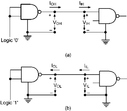
It may be mentioned here that the direction of the LOW-level input and output currents shown in Fig. 3(b) is applicable to logic families with current-sinking action such as TTL.
Supply current, ICC. The supply current when the output is HIGH, LOW and in the high-impedance state is respectively designated as ICCH, ICCL and ICCZ.
Rise time, tr. This is the time that elapses between 10 and 90 % of the final signal level when the signal is making a transition from logic LOW to logic HIGH.
Fall time, tf . This is the time that elapses between 90 and 10 % of the signal level when it is making HIGH to LOW transition.
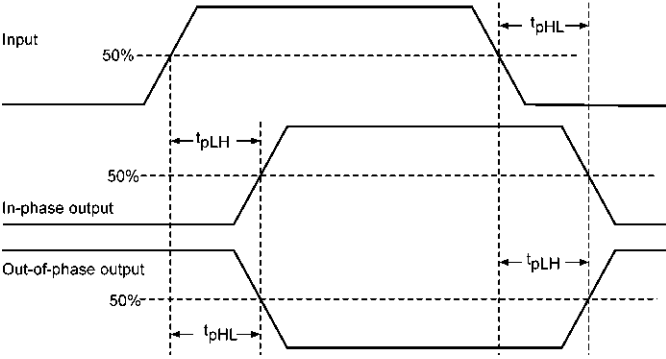
Propagation delay tp. The propagation delay is the time delay between the occurrence of change in the logical level at the input and before it is reflected at the output. It is the time delay between the specified voltage points on the input and output waveforms.
Propagation delays are separately defined for LOW-to-HIGH and HIGH-to-LOW transitions at the output. In addition, we also define enable and disable time delays that occur during transition between the high-impedance state and defined logic LOW or HIGH states.
Propagation delay tpLH. This is the time delay between specified voltage points on the input and output waveforms with the output changing from LOW to HIGH.
Propagation delay tpHL. This is the time delay between specified voltage points on the input and output waveforms with the output changing from HIGH to LOW. Figure 4 shows the two types of propagation delay parameter.
Disable time from the HIGH state, tpHZ. Defined for a tristate device, this is the time delay between specified voltage points on the input and output waveforms with the tristate output changing from the logic HIGH level to the high-impedance state.
Disable time from the LOW state, tpLZ. Defined for a tristate device, this is the time delay between specified voltage points on the input and output waveforms with the tristate output changing from the logic LOW level to the high-impedance state.
Enable time from the HIGH state, tpZH. Defined for a tristate device, this is the time delay between specified voltage points on the input and output waveforms with the tristate output changing from the high-impedance state to the logic HIGH level.
Enable time from the LOW state, tpZL. Defined for a tristate device, this is the time delay between specified voltage points on the input and output waveforms with the tristate output changing from the high-impedance state to the logic LOW level.
Maximum clock frequency, fmax. This is the maximum frequency at which the clock input of a flip-flop can be driven through its required sequence while maintaining stable transitions of logic level at the output in accordance with the input conditions and the product specification. It is also referred to as the maximum toggle rate for a flip-flop or counter device.
Power dissipation. The power dissipation parameter for a logic family is specified in terms of power consumption per gate and is the product of supply voltage VCC and supply current ICC. The supply current is taken as the average of the HIGH-level supply current ICCH and the LOW-level supply current ICCL.
Characteristics Parameters of Logic Families
Speed–power product. The speed of a logic circuit can be increased, that is, the propagation delay can be reduced, at the expense of power dissipation.
We will recall that, when a bipolar transistor switches between cut-off and saturation, it dissipates the least power but has a large associated switching time delay. On the other hand, when the transistor is operated in the active region, power dissipation goes up while the switching time decreases drastically.
It is always desirable to have in a logic family low values for both propagation delay and power dissipation parameters.
A useful figure-of-merit used to evaluate different logic families is the speed–power product, expressed in picojoules, which is the product of the propagation delay (measured in nanoseconds) and the power dissipation per gate (measured in milliwatts).
Fan-out. The fan-out is the number of inputs of a logic function that can be driven from a single output without causing any false output. It is a characteristic of the logic family to which the device belongs. It can be computed from IOH/IIH in the logic HIGH state and from IOL/IIL in the logic LOW state.
If, in a certain case, the two values IOH/IIH and IOL/IIL are different, the fan-out is taken as the smaller of the two.
This description of the fan-out is true for bipolar logic families like TTL and ECL. When determining the fan-out of CMOS logic devices, we should also take into consideration how much input load capacitance can be driven from the output without exceeding the acceptable value of propagation delay.
Noise margin. This is a quantitative measure of noise immunity offered by the logic family. When the output of a logic device feeds the input of another device of the same family, a legal HIGH logic state at the output of the feeding device should be treated as a legal HIGH logic state by the input of the device being fed.
Similarly, a legal LOW logic state of the feeding device should be treated as a legal LOW logic state by the device being fed. We have seen in earlier paragraphs while defining important characteristic parameters that legal HIGH and LOW voltage levels for a given logic family are different for outputs and inputs.
Figure 5 shows the generalized case of legal HIGH and LOW voltage levels for output [Fig. 5(a)] and input [Fig. 5(b)]. As we can see from the two diagrams, there is a disallowed range of output voltage levels from VOL(max.) to VOH(min.) and an indeterminate range of input voltage levels from VIL(max.) to VIH(min.).

Since VIL(max.) is greater than VOL(max.), the LOW output state can therefore tolerate a positive voltage spike equal to VIL(max.) − VOL(max.) and still be a legal LOW input.
Similarly, VOH(min.) is greater than VIH (min.), and the HIGH output state can tolerate a negative voltage spike equal to VOH(min.) − VIH (min.) and still be a legal HIGH input. Here, VIL(max.) − VOL(max.) and VOH(min.) − VIH (min.) are respectively known as the LOW-level and HIGH-level noise margin.
Let us illustrate it further with the help of data for the standard TTL family. The minimum legal HIGH output voltage level in the case of the standard TTL is 2.4 V. Also, the minimum legal HIGH input voltage level for this family is 2 V. This implies that, when the output of one device feeds the input of another, there is an available margin of 0.4 V. That is, any negative voltage spikes of amplitude less than or equal to 0.4 V on the signal line do not cause any spurious transitions.
Similarly, when the output is in the logic LOW state, the maximum legal LOW output voltage level in the case of the standard TTL is 0.4 V. Also, the maximum legal LOW input voltage level for this family is 0.8 V. This implies that, when the output of one device feeds the input of another, there is again an available margin of 0.4 V.
That is, any positive voltage spikes of amplitude less than or equal to 0.4 V on the signal line do not cause any spurious transitions. This leads to the standard TTL family offering a noise margin of 0.4 V.
To generalize, the noise margin offered by a logic family, as outlined earlier, can be computed from the HIGH-state noise margin, VNH = VOH(min.) − VIH(min.), and the LOW-state noise margin, VNL = VIL(max.) − VOL(max.). If the two values are different, the noise margin is taken as the lower of the two.
Related Posts
- Logic Gates
- Significance & Types of Logic Family
- Characteristics Parameters of Logic Families
- TTL Logic Family
- ECL Logic Family
- CMOS Logic Family
- Interfacing of Logic Families
- Microcontroller Architecture
- Components of Microcontroller
- Interfacing Devices with Microcontroller
- IC Based Multivibrator Circuits
- Astable, Monostable & Bistable Multivibrator
- Logic Analyser
- Types of Oscilloscope
- Frequency Synthesizers
- Frequency Counter