Digital integrated circuits are produced using several different circuit configurations and production technologies. Each such approach is called a specific logic family. In this article, we will discuss different logic families used to hardware-implement different logic functions in the form of digital integrated circuits.
There are a variety of circuit configurations or more appropriately various approaches used to produce different types of digital integrated circuit. Each such fundamental approach is called a logic family.
The idea is that different logic functions, when fabricated in the form of an IC with the same approach, or in other words belonging to the same logic family, will have identical electrical characteristics. These characteristics include supply voltage range, speed of response, power dissipation, input and output logic levels, current sourcing and sinking capability, fan-out, noise margin, etc.
In other words, the set of digital ICs belonging to the same logic family are electrically compatible with each other.
Significance of Logic Family
A digital system in general comprises digital ICs performing different logic functions, and choosing these ICs from the same logic family guarantees that different ICs are compatible with respect to each other and that the system as a whole performs the intended logic function.
In the case where the output of an IC belonging to a certain family feeds the inputs of another IC belonging to a different family, we must use established interface techniques to ensure compatibility.
Understanding the features and capabilities of different logic families is very important for a logic designer who is out to make an optimum choice for his new digital design from the available logic family alternatives. A not so well thought out choice can easily underkill or overkill the design with either inadequate or excessive capabilities.
Types of Logic Family
The entire range of digital ICs is fabricated using either bipolar devices or MOS devices or a combination of the two.
Different logic families falling in the first category are called bipolar families, and these include
- diode logic (DL),
- resistor transistor logic (RTL),
- diode transistor logic (DTL),
- transistor transistor logic (TTL),
- emitter coupled logic (ECL), also known as current mode logic (CML), and
- integrated injection logic (I2L).
The logic families that use MOS devices as their basis are known as MOS families, and the prominent members belonging to this category are the
- PMOS family (using P-channel MOSFETs),
- the NMOS family (using N-channel MOSFETs) and
- the CMOS family (using both N- and P-channel devices).
The Bi-MOS logic family uses both bipolar and MOS devices.
Of all the logic families listed above, the first three, that is, diode logic (DL), resistor transistor logic (RTL) and diode transistor logic (DTL), are of historical importance only. Diode logic used diodes and resistors and in fact was never implemented in integrated circuits. The RTL family used resistors and bipolar transistors, while the DTL family used resistors, diodes and bipolar transistors.
Both RTL and DTL suffered from large propagation delay owing to the need for the transistor base charge to leak out if the transistor were to switch from conducting to non-conducting state.
The DL, RTL and DTL families, however, were rendered obsolete very shortly after their introduction in the early 1960s owing to the arrival on the scene of transistor transistor logic (TTL). Logic families that are still in widespread use include TTL, CMOS, ECL, NMOS and Bi-CMOS.
The PMOS and I2L logic families, which were mainly intended for use in custom large-scale integrated (LSI) circuit devices, have also been rendered more or less obsolete, with the NMOS logic family replacing them for LSI and VLSI applications.
Transistor Transistor Logic (TTL)
TTL stands for transistor transistor logic. It is a logic family implemented with bipolar process technology that combines or integrates NPN transistors, PN junction diodes and diffused resistors in a single monolithic structure to get the desired logic function. The NAND gate is the basic building block of this logic family.
TTL Subfamilies: The TTL family has a number of subfamilies including standard TTL, low-power TTL, high-power TTL, low-power Schottky TTL, Schottky TTL, advanced low-power Schottky TTL, advanced Schottky TTL and fast TTL.
The ICs belonging to the TTL family are designated as 74 or 54 (for standard TTL), 74L or 54L (for low-power TTL), 74H or 54H (for high-power TTL), 74LS or 54LS (for low-power Schottky TTL), 74S or 54S (for Schottky TTL), 74ALS or 54ALS (for advanced low-power Schottky TTL), 74AS or 54AS (for advanced Schottky TTL) and 74F or 54F (for fast TTL).
An alphabetic code preceding this indicates the name of the manufacturer (DM for National Semiconductors, SN for Texas Instruments and so on). A two-, three- or four-digit numerical code tells the logic function performed by the IC.
It may be mentioned that 74-series devices and 54-series devices are identical except for their operational temperature range. The 54-series devices are MIL-qualified (operational temperature range: −55 °C to +125 °C) versions of the corresponding 74-series ICs (operational temperature range: 0 °C to 70 °C). For example, 7400 and 5400 are both quad two-input NAND gates.
To get more information about TTL logic family, please follow the link.
Emitter Coupled Logic (ECL)
The ECL family is the fastest logic family in the group of bipolar logic families. The characteristic features that give this logic family its high speed or short propagation delay.
ECL Subfamilies: The first monolithic emitter coupled logic family was introduced by ON Semiconductor, formerly a division of Motorola, with the MECL-I series of devices in 1962, with the MECL-II series following it up in 1966. Both these logic families have become obsolete.
Currently, popular subfamilies of ECL logic include MECL-III (also called the MC 1600 series), the MECL-10K series, the MECL-10H series and the MECL-10E series (ECLinPS and ECLinPSLite). The MECL-10K series further divided into the 10 100-series and 10 200-series devices.
To get more information about ECL logic family, please follow the link.
CMOS Logic Family
The CMOS (Complementary Metal Oxide Semiconductor) logic family uses both N-type and P-type MOSFETs (enhancement MOSFETs, to be more precise) to realize different logic functions. The two types of MOSFET are designed to have matching characteristics. That is, they exhibit identical characteristics in switch-OFF and switch-ON conditions.
The main advantage of the CMOS logic family over bipolar logic families discussed so far lies in its extremely low power dissipation, which is near-zero in static conditions. In fact, CMOS devices draw power only when they are switching. This allows integration of a much larger number of CMOS gates on a chip than would have been possible with bipolar or NMOS (to be discussed later) technology.
CMOS technology today is the dominant semiconductor technology used for making microprocessors, memory devices and application-specific integrated circuits (ASICs).
CMOS Subfamilies: The popular CMOS subfamilies include the 4000A, 4000B, 4000UB, 54/74C, 54/74HC, 54/74HCT, 54/74AC and 54/74ACT families. The 4000A CMOS family has been replaced by its high-voltage versions in the 4000B and 4000UB CMOS families, with the former having buffered and the latter having un-buffered outputs. 54/74C, 54/74HC, 54/74HCT, 54/74AC and 54/74ACT are CMOS logic families with pin-compatible 54/74 TTL series logic functions.
To get more information about CMOS logic family, please follow the link.
BiCMOS Logic Family
The BiCMOS logic family integrates bipolar and CMOS devices on a single chip with the objective of deriving the advantages individually present in bipolar and CMOS logic families.
While bipolar logic families such as TTL and ECL have the advantages of faster switching speed and larger output drive current capability, CMOS logic scores over bipolar counterparts when it comes to lower power dissipation, higher noise margin and larger packing density.
BiCMOS logic attempts to get the best of both worlds. Two major categories of BiCMOS logic devices have emerged over the years since its introduction in 1985.
In one type of device, moderate-speed bipolar circuits are combined with high-performance CMOS circuits. Here, CMOS circuitry continues to provide low power dissipation and larger packing density. Selective use of bipolar circuits gives improved performance.
In the other category, the bipolar component is optimized to produce high-performance circuitry. In the following paragraphs, we will briefly describe the basic BiCMOS inverter and NAND circuits.
BiCMOS Inverter: Figure 1 shows the internal schematic of a basic BiCMOS inverter. When the input is LOW, N-channel MOSFETs Q2 and Q3 are OFF. P-channel MOSFET Q1 and N-channel MOSFET Q4 are ON.
This leads transistors Q5 and Q6 to be in the ON and OFF states respectively. Transistor Q6 is OFF because it does not get the required forward-biased base-emitter voltage owing to a conducting Q4.
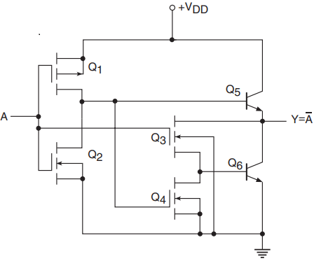
Conducting Q5 drives the output to a HIGH state, sourcing a large drive current to the load. The HIGH-state output voltage is given by the equation
VOH = VDD −VBE(Q5)
When the input is driven to a HIGH state, Q2 and Q3 turn ON. Initially, Q4 is also ON and the output discharges through Q3 and Q4. When Q4 turns OFF owing to its gate-source voltage falling below the required threshold voltage, the output continues to discharge until the output voltage equals the forward-biased base-emitter voltage drop of Q6 in the active region.
The LOW-state output voltage is given by the equation
VOL = VBE(Q6 in active mode) = 0.7V
BiCMOS NAND: Figure 2 shows the internal schematic of a two-input NAND in BiCMOS logic. The operation of this circuit can be explained on similar lines to the case of an inverter.
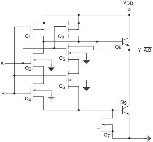
Note that MOSFETs Q1–Q4 constitute a two-input NAND in CMOS. Also note the similarity of this circuit to the one shown in Fig. 1. The CMOS inverter stage of Fig. 1 is replaced by CMOS NAND in Fig. 2. N-channel MOSFET Q3 in Fig. 1 is replaced by a series connection of N-channel MOSFETs Q5 and Q6 to accommodate the two inputs.
The HIGH-state and LOW-state output voltage levels of this circuit are given by the equations
VOH = (VDD − 0.7)
VOL = 0.7
NMOS and PMOS Logic
Logic families discussed so far are the ones that are commonly used for implementing discrete logic functions such as logic gates, flip-flops, counters, multiplexers, demultiplexers, etc., in relatively less complex digital ICs belonging to the small-scale integration (SSI) and medium-scale integration (MSI) level of inner circuit complexities.
The TTL, the CMOS and the ECL logic families are not suitable for implementing digital ICs that have a large-scale integration (LSI) level of inner circuit complexity and above. The competitors for LSI-class digital ICs are the PMOS, the NMOS and the integrated injection logic (I2L). The first two are briefly discussed in this section, and the third is discussed in next Section.
PMOS Logic: The PMOS logic family uses P-channel MOSFETS. Figure 3(a) shows an inverter circuit using PMOS logic. MOSFET Q1 acts as an active load for the MOSFET switch Q2. For the circuit shown, GND and −VDD respectively represent a logic ‘1’ and a logic ‘0’ for a positive logic system.
When the input is grounded (i.e. logic ‘1’), Q2 remains in cut-off and −VDD appears at the output through the conducting Q1. When the input is at −VDD or near −VDD, Q2 conducts and the output goes to near-zero potential (i.e. logic ‘1’).
Figure 3(b) shows a PMOS logic based two-input NOR gate. In the logic arrangement of Fig. 3(b), the output goes to logic ‘1’ state (i.e. ground potential) only when both Q1 and Q2 are conducting. This is possible only when both the inputs are in logic ‘0’ state.
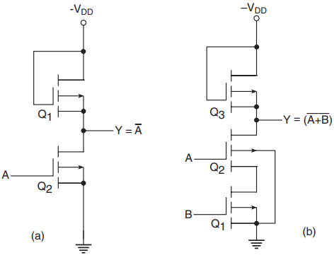
For all other possible input combinations, the output is in logic ‘0’ state, because, with either Q1 or Q2 non-conducting, the output is nearly −VDD through the conducting Q3. The circuit of Fig. 3(b) thus behaves like a two-input NOR gate in positive logic.
It may be mentioned here that the MOSFET being used as load [Q1 in Fig. 3(a) and Q3 in Fig. 3(b)] is designed so as to have an ON-resistance that is much greater than the total ON-resistance of the MOSFETs being used as switches [Q2 in Fig. 3(a) and Q1 and Q2 in Fig. 3(b)].
NMOS Logic: The NMOS logic family uses N-channel MOSFETS. N-channel MOS devices require a smaller chip area per transistor compared with P-channel devices, with the result that NMOS logic offers a higher density.
Also, owing to the greater mobility of the charge carriers in N-channel devices, the NMOS logic family offers higher speed too. It is for this reason that most of the MOS memory devices and microprocessors employ NMOS logic or some variation of it such as VMOS, DMOS and HMOS. VMOS, DMOS and HMOS are only structural variations of NMOS, aimed at further reducing the propagation delay.
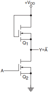
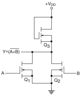
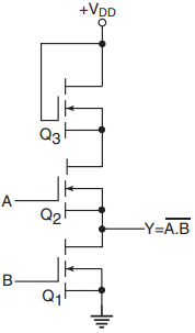
Figures 4(a), (b) and (c) respectively show an inverter, a two-input NOR and a two-input NAND using NMOS logic. The logic circuits are self-explanatory.
Integrated Injection Logic (I2L)
Family Integrated injection logic (I2L), also known as current injection logic, is well suited to implementing LSI and VLSI digital functions and is a close competitor to the NMOS logic family.
Figure 5 shows the basic I2L family building block, which is a multi-collector bipolar transistor with a current source driving its base. Transistors Q3 and Q4 constitute current sources. The magnitude of current depends upon externally connected R and applied +V. This current is also known as the injection current, which gives it its name of injection logic.
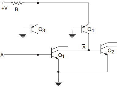
If input A is HIGH, the injection current through Q3 flows through the base-emitter junction of Q1. Transistor Q1 saturates and its collector drops to a low voltage, typically 50–100 mV. When A is LOW, the injection current is swept away from the base-emitter junction of Q1. Transistor Q1 becomes open and the injection current through Q4 saturates Q2, with the result that the Q1 collector potential equals the base-emitter saturation voltage of Q2, typically 0.7 V.
The speed of I2L family devices is a function of the injection current I and improves with increase in current, as a higher current allows a faster charging of capacitive loads present at bases of transistors.
The programmable injection current feature is made use of in the I2L family of digital ICs to choose the desired speed depending upon intended application. The logic ‘0’ level is VCE(sat.) of the driving transistor (Q1 in the present case), and the logic ‘1’ level is VBE(sat.) of the driven transistor (Q2 in the present case). Typically, the logic ‘0’ and logic ‘1’ levels are 0.1 and 0.7 V respectively. The speed–power product of the I2L family is typically under 1 pJ.
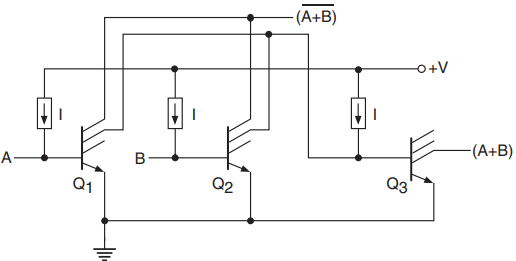
Multiple collectors of different transistors can be connected together to form wired logic. Figure 6 shows one such arrangement, depicting the generation of OR and NOR outputs of two logic variables A and B.
Related Posts
- Logic Gates
- Significance & Types of Logic Family
- Characteristics Parameters of Logic Families
- TTL Logic Family
- ECL Logic Family
- CMOS Logic Family
- Interfacing of Logic Families
- Microcontroller Architecture
- Components of Microcontroller
- Interfacing Devices with Microcontroller
- IC Based Multivibrator Circuits
- Astable, Monostable & Bistable Multivibrator
- Logic Analyser
- Types of Oscilloscope
- Frequency Synthesizers
- Frequency Counter