Logic Analyser
The logic analyser is used for performance analysis and fault diagnosis of digital systems. Logic analysers have become a very relevant and indispensable diagnostic tool in the present day instrumentation scenario, with the whole gamut of electronic instruments being centred on microprocessor/microcomputer based digital architecture.
In addition, most logic analysers can be configured to format their outputs as a sequence of microprocessor instructions, which makes them useful for debugging software too.
Operational Modes of Logic Analyser
The logic analyser works in one of two modes of operation, namely the asynchronous timing mode and the synchronous state mode. A brief description of each of these two modes is given in the following paragraphs.
Asynchronous Timing Mode: In this mode of operation, the signals being probed are recorded either as logic ‘0’ or logic ‘1’. The logic analyser provides the time base referred to as the ‘internal clock. The time base determines when data values are clocked into the memory of the analyser.
On screen, the asynchronous mode display looks similar to an oscilloscope display except for the number of channels that can be displayed, which is much larger in the case of a logic analyser.
Synchronous State Mode: In this mode of operation, samples of signals are stored in the memory on a clock edge, referred to as the external clock, supplied by the system under investigation. The logic analyser samples new data values or states only when directed by the clock signal.
On a given clock edge, the logic states of various signals constitute a group. The logic analyser display in this mode shows progression of states represented by these groups.
Logic Analyser Architecture
Figure 1 shows the block schematic arrangement of a logic analyser. Important constituents of all logic analysers include probes, memory, trigger generator, clock generator, storage qualifier and user interface.
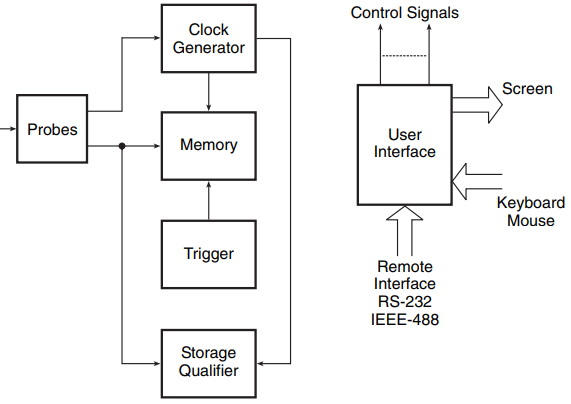
Probes: Probes are used to provide physical connection to the circuit under test without causing any loading effects, so that the logic signal of interest is not unduly affected and its timing integrity is maintained. The probes usually operate as voltage dividers.
By this, the comparators inside the probe are asked to handle the lowest possible voltage slew rate that enables higher-speed signals to be captured. These comparators have an adjustable threshold to make the probes compatible with different logic families as different families have different voltage thresholds. The comparators transform the input signals into logic ls and 0s.
Memory: The memory stores the sampled logic values. Addresses for given samples are supplied internally. In a typical measurement using a logic analyser, the user is interested in observing the logic signals around some event called the measurement trigger and the samples have a timing relationship with this trigger event. These samples are placed in the memory, depending upon the instantaneous value of the internally supplied address.
Trigger: Logic analysers have both a combinational (or word-recognized) trigger mode and an external trigger mode. In the combinational trigger mode, the trigger circuitry compares the incoming data with a word programmed by the user from the front panel. A trigger signal is generated when the incoming data match with the programmed word.
Data are being sampled and stored in the memory by either an internal or an external clock. On the occurrence of a trigger, the stored data samples are displayed on the screen.
Clock Generator: As stated earlier, the clock is either internal or external, depending upon whether the selected operational mode is the asynchronous timing mode or the synchronous state mode. The two modes are described earlier.
Again, in the timing mode there are two commonly used approaches. Some logic analysers offer both approaches. In the first approach, called the continuous storage mode, the clock is generated at the selected rate irrespective of the activity occurring on the input signals. The logic status of the input signal is stored in the memory on every clock cycle [Fig. 2(a)].
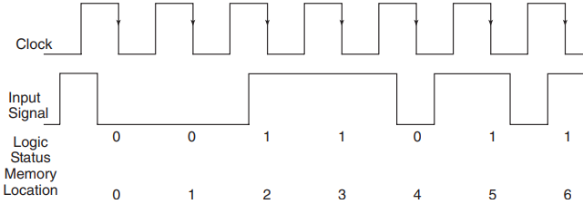
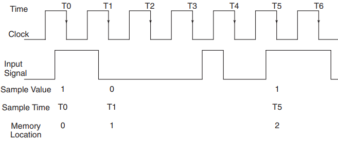
In the second approach, called the transitional timing mode, the input signals are again sampled at the selected rate, but the clock generator circuitry allows the samples to be stored in the memory only if one or more signals change their logic status. Thus, the memory storage locations are used only if inputs change, leading to more efficient use of memory.
For each sample, however, a time marker is recorded, as shown in Fig. 2(b). This approach offers a distinct advantage when long time records of infrequent or bursts of finely timed events are to be recorded.
Storage Qualifier: The function of the storage qualifier is to determine which data samples are clocked into the memory. The storage qualifier block looks at the sampled data and tests them against a criterion. If the criterion is met, the clocked sample is stored in the memory. This feature is particularly useful in troubleshooting microprocessor architectures.
For instance, if the circuit under test is a microprocessor bus, this function can be used to separate bus cycles to a specific I/O port from cycles to all other ports or from instruction cycles.
User Interface: Benchtop logic analysers typically use a dedicated keyboard and CRT display. Graphical user interfaces (GUIs) similar to those available on personal computers are also available with many products. Also, interfaces such as RS-232, IEEE-488 or local area network (LAN) enable the use of the instrument from a personal computer or a workstation.
Remote interfaces are important in manufacturing applications. LAN interfaces have emerged as critical links in research and development activities where these instruments can be tied to project databases.
Key Specifications of Logic Analyser
Some of the important specifications of logic analysers include sample rate, set-up and hold times, probe loading, memory depth and channel count. Trigger resources, the availability of preprocessors/inverse assemblers, nonvolatile storage and the ability of the logic analyser to store time value along with captured data are the other key features.
Sample rate: The sample rate in the timing mode determines the minimum resolvable time interval. Since the relationship of the sample clock and the input signal transition is random, two edges of the same signal can be measured to an accuracy of two sample periods.
Measuring a transition on one signal with respect to a transition on another signal can also be done with an accuracy of two sample periods plus whatever skew exists between the channels. In the state mode, the sample rate determines the maximum clock rate that can be measured in the target state machine.
Set-up and Hold Times: The set-up and hold time specification in the case of logic analysers is similar to that in the case of flip-flops, registers and memory devices. Like these devices, a logic analyser also needs stable data for a specified time before the clock becomes active. This specified time is the set-up time.
The hold time is the time interval for which the data must be held after the active transition of the clock to enable data capture. The hold time is typically zero for logic analysers.
Probe Loading: It is desired that the target system not be perturbed by probe loading. Logic analysers with a sampling rate of equal to or less than 500 MHz have probe specifications of typically 100K and 6 – 8 pF. Analysers having a sample rate greater than 1 GHz usually come with SPICE models for their probes so as to enable the users to know the true impact of probe loading on signal integrity.
Memory depth: The memory depth determines the maximum time window that can be captured in the timing mode or the total number of states or bus cycles that can be captured in the state mode. Most of the logic analysers offer 4K to 1M samples of memory.
Channel count: Channel count is the number of available input channels. Together with maximum rate, channel count determines the cost of instrument.
Related Posts
- Logic Gates
- Significance & Types of Logic Family
- Characteristics Parameters of Logic Families
- TTL Logic Family
- ECL Logic Family
- CMOS Logic Family
- Interfacing of Logic Families
- Microcontroller Architecture
- Components of Microcontroller
- Interfacing Devices with Microcontroller
- IC Based Multivibrator Circuits
- Astable, Monostable & Bistable Multivibrator
- Logic Analyser
- Types of Oscilloscope
- Frequency Synthesizers
- Frequency Counter