Logic Gates
Logic gates are electronic circuits that can be used to implement the most elementary logic expressions, also known as Boolean expressions. The logic gate is the most basic building block of combinational logic. There are three basic logic gates, namely the OR gate, the AND gate and the NOT gate. Other logic gates that are derived from these basic gates are the NAND gate, the NOR gate, the EXCLUSIVE-OR gate and the EXCLUSIVE-NOR gate.
This article deals with logic gates and some related devices such as buffers, drivers, etc., as regards their basic functions. The treatment of the subject matter is mainly with the help of respective truth tables and Boolean expressions.
Positive and Negative Logic
The binary variables, as we know, can have either of the two states, i.e. the logic ‘0’ state or the logic ‘1’ state. These logic states in digital systems such as computers, for instance, are represented by two different voltage levels or two different current levels. If the more positive of the two voltage or current levels represents a logic ‘1’ and the less positive of the two levels represents a logic ‘0’, then the logic system is referred to as a positive logic system.
If the more positive of the two voltage or current levels represents a logic ‘0’ and the less positive of the two levels represents a logic ‘1’, then the logic system is referred to as a negative logic system. The following examples further illustrate this concept.
If the two voltage levels are 0 V and +5 V, then in the positive logic system the 0 V represents a logic ‘0’ and the +5 V represents a logic ‘1’. In the negative logic system, 0 V represents a logic ‘1’ and +5 V represents a logic ‘0’. If the two voltage levels are 0 V and −5 V, then in the positive logic system the 0 V represents a logic ‘1’ and the −5 V represents a logic ‘0’. In the negative logic system, 0 V represents a logic ‘0’ and −5 V represents a logic ‘1’.
It is interesting to note, as we will discover in the latter part of the article, that a positive OR is a negative AND. That is, OR gate hardware in the positive logic system behaves like an AND gate in the negative logic system. The reverse is also true. Similarly, a positive NOR is a negative NAND, and vice versa.
Logic Gate Truth Table
A truth table lists all possible combinations of input binary variables and the corresponding outputs of a logic system. The logic system output can be found from the logic expression, often referred to as the Boolean expression, that relates the output with the inputs of that very logic system.
When the number of input binary variables is only one, then there are only two possible inputs, i.e. ‘0’ and ‘1’. If the number of inputs is two, there can be four possible input combinations, i.e. 00, 01, 10 and 11.
Figure1(b) shows the truth table of the two-input logic system represented by Fig. 1(a). The logic system of Fig. 4.1(a) is such that Y = 0 only when both A = 0 and B = 0. For all other possible input combinations, output Y = 1.
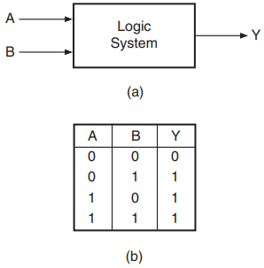
Similarly, for three input binary variables, the number of possible input combinations becomes eight, i.e. 000, 001, 010, 011, 100, 101, 110 and 111. This statement can be generalized to say that, if a logic circuit has n binary inputs, its truth table will have 2n possible input combinations, or in other words 2n rows.
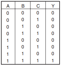
Figure 2 shows the truth table of a three-input logic circuit, and it has 8 (= 23) rows. Incidentally, as we will see later in the chapter, this is the truth table of a three-input AND gate.
It may be mentioned here that the truth table of a three-input AND gate as given in Fig. 2 is drawn following the positive logic system, and also that, in all further discussion throughout the article, we will use a positive logic system unless otherwise specified.
Basic Logic Gates
The logic gate is the most basic building block of any digital system, including computers. Each one of the basic logic gates is a piece of hardware or an electronic circuit that can be used to implement some basic logic expression. While laws of Boolean algebra could be used to do manipulation with binary variables and simplify logic expressions, these are actually implemented in a digital system with the help of electronic circuits called logic gates. The three basic logic gates are the OR gate, the AND gate and the NOT gate.
OR Gate: An OR gate performs an ORing operation on two or more than two logic variables. The OR operation on two independent logic variables A and B is written as Y = A+B and reads as Y equals A OR B and not as A plus B. An OR gate is a logic circuit with two or more inputs and one output.
The output of an OR gate is LOW only when all of its inputs are LOW. For all other possible input combinations, the output is HIGH. This statement when interpreted for a positive logic system means the following. The output of an OR gate is a logic ‘0’ only when all of its inputs are at logic ‘0’. For all other possible input combinations, the output is a logic ‘1’.

Figure 3 shows the circuit symbol and the truth table of a two-input OR gate. The operation of a two-input OR gate is explained by the logic expression
Y = A+B
As an illustration, if we have four logic variables and we want to know the logical output of A + B + C + D, then it would be the output of a four-input OR gate with A, B, C and D as its inputs.
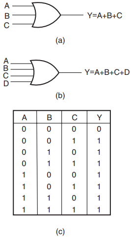
Figures 4(a) and (b) show the circuit symbol of three-input and four-input OR gates. Figure 4(c) shows the truth table of a three-input OR gate. Logic expressions explaining the functioning of three-input and four-input OR gates are Y = A+B +C and Y = A+B +C +D.
AND Gate: An AND gate is a logic circuit having two or more inputs and one output. The output of an AND gate is HIGH only when all of its inputs are in the HIGH state. In all other cases, the output is LOW. When interpreted for a positive logic system, this means that the output of the AND gate is a logic ‘1’ only when all of its inputs are in logic ‘1’ state. In all other cases, the output is logic ‘0’.
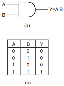
The logic symbol and truth table of a two-input AND gate are shown in Figs 5(a) and (b) respectively.
Figures 6(a) and (b) show the logic symbols of three-input and four-input AND gates respectively. Figure 6(c) gives the truth table of a four-input AND gate.
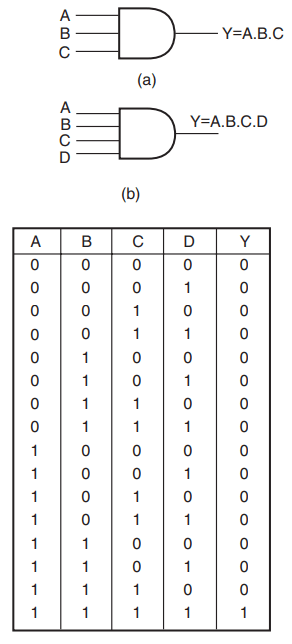
The AND operation on two independent logic variables A and B is written as Y = A.B and reads as Y equals A AND B and not as A multiplied by B.
Here, A and B are input logic variables and Y is the output. An AND gate performs an ANDing operation:
- for a two-input AND gate, Y = A.B;
- for a three-input AND gate, Y = A.B.C;
- for a four-input AND gate, Y = A.B.C.D.
If we interpret the basic definition of OR and AND gates for a negative logic system, we have an interesting observation. We find that an OR gate in a positive logic system is an AND gate in a negative logic system. Also, a positive AND is a negative OR.
NOT Gate: A NOT gate is a one-input, one-output logic circuit whose output is always the complement of the input. That is, a LOW input produces a HIGH output, and vice versa.
When interpreted for a positive logic system, a logic ‘0’ at the input produces a logic ‘1’ at the output, and vice versa.
It is also known as a ‘complementing circuit’ or an ‘inverting circuit’. Figure 7 shows the circuit symbol and the truth table.
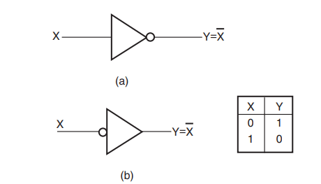
The NOT operation on a logic variable X is denoted as Xbar or X’ . That is, if X is the input to a NOT circuit, then its output Y is given by Y = X or X and reads as Y equals NOT X. Thus, if X = 0, Y = 1 and if X = 1, Y = 0.
EXCLUSIVE-OR Gate: The EXCLUSIVE-OR gate, commonly written as EX-OR gate, is a two-input, one-output gate. Figures 8(a) and (b) respectively show the logic symbol and truth table of a two-input EX-OR gate.
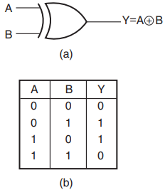
As can be seen from the truth table, the output of an EX-OR gate is a logic ‘1’ when the inputs are unlike and a logic ‘0’ when the inputs are like.
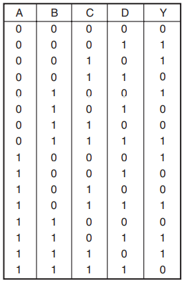
Although EX-OR gates are available in integrated circuit form only as two-input gates, unlike other gates which are available in multiple inputs also, multiple-input EX-OR logic functions can be implemented using more than one two-input gates. The truth table of a multiple-input EX-OR function can be expressed as follows.
The output of a multiple-input EX-OR logic function is a logic ‘1’ when the number of 1s in the input sequence is odd and a logic ‘0’ when the number of 1s in the input sequence is even, including zero. That is, an all 0s input sequence also produces a logic ‘0’ at the output. Figure 8(c) shows the truth table of a four-input EX-OR function.
The output of a two-input EX-OR gate is expressed by

NAND Gate: NAND stands for NOT AND. An AND gate followed by a NOT circuit makes it a NAND gate [Fig. 9(a)]. Figure 9(b) shows the circuit symbol of a two-input NAND gate. The truth table of a NAND gate is obtained from the truth table of an AND gate by complementing the output entries [Fig. 9(c)].
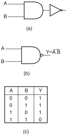
The output of a NAND gate is a logic ‘0’ when all its inputs are a logic ‘1’. For all other input combinations, the output is a logic ‘1’. NAND gate operation is logically expressed as

In general, the Boolean expression for a NAND gate with more than two inputs can be written as

NOR Gate: NOR stands for NOT OR. An OR gate followed by a NOT circuit makes it a NOR gate [Fig. 10(a)]. The truth table of a NOR gate is obtained from the truth table of an OR gate by complementing the output entries.
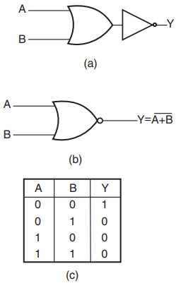
The output of a NOR gate is a logic ‘1’ when all its inputs are logic ‘0’. For all other input combinations, the output is a logic ‘0’.
The output of a two-input NOR gate is logically expressed as

In general, the Boolean expression for a NOR gate with more than two inputs can be written as

EXCLUSIVE-NOR Gate: EXCLUSIVE-NOR (commonly written as EX-NOR) means NOT of EX-OR, i.e. the logic gate that we get by complementing the output of an EX-OR gate.
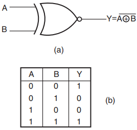
Figure 11 shows its circuit symbol along with its truth table. The truth table of an EX-NOR gate is obtained from the truth table of an EX-OR gate by complementing the output entries. Logically,

The output of a two-input EX-NOR gate is a logic ‘1’ when the inputs are like and a logic ‘0’ when they are unlike. In general, the output of a multiple-input EX-NOR logic function is a logic ‘0’ when the number of 1s in the input sequence is odd and a logic ‘1’ when the number of 1s in the input sequence is even including zero. That is, an all 0s input sequence also produces a logic ‘1’ at the output.
INHIBIT Gate: There are many situations in digital circuit design where the passage of a logic signal needs to be either enabled or inhibited depending upon certain other control inputs. INHIBIT here means that the gate produces a certain fixed logic level at the output irrespective of changes in the input logic level.
As an illustration, if one of the inputs of a four-input NOR gate is permanently tied to logic ‘1’ level, then the output will always be at logic ‘0’ level irrespective of the logic status of other inputs. This gate will behave as a NOR gate only when this control input is at logic ‘0’ level. This is an example of the INHIBIT function.
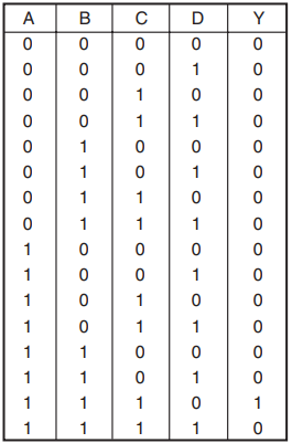
The INHIBIT function is available in integrated circuit form for an AND gate, which is basically an AND gate with one of its inputs negated by an inverter. The negated input acts to inhibit the gate.
In other words, the gate will behave like an AND gate only when the negated input is driven to a logic ‘0’. Figure 12 shows the circuit symbol and truth table of a four-input INHIBIT gate.

Universal Logic Gates
OR, AND and NOT gates are the three basic logic gates as they together can be used to construct the logic circuit for any given Boolean expression. NOR and NAND gates have the property that they individually can be used to hardware-implement a logic circuit corresponding to any given Boolean expression.
That is, it is possible to use either only NAND gates or only NOR gates to implement any Boolean expression. This is so because a combination of NAND gates or a combination of NOR gates can be used to perform functions of any of the basic logic gates. It is for this reason that NAND and NOR gates are universal gates.
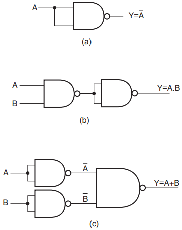
As an illustration, Fig. 13 shows how two-input NAND gates can be used to construct a NOT circuit [Fig. 13(a)], a two-input AND gate [Fig. 13(b)] and a two-input OR gate [Fig. 13(c)]. Figure 14 shows the same using NOR gates.
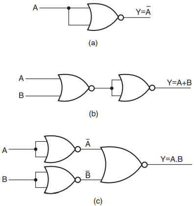
Understanding the conversion of NAND to OR and NOR to AND requires the use of DeMorgan’s theorem.
Logic Gates with Open Collector/Drain Outputs
These are gates where we need to connect an external resistor, called the pull-up resistor, between the output and the DC power supply to make the logic gate perform the intended logic function. Depending on the logic family used to construct the logic gate, they are referred to as gates with open collector output (in the case of the TTL logic family) or open drain output (in the case of the MOS logic family).
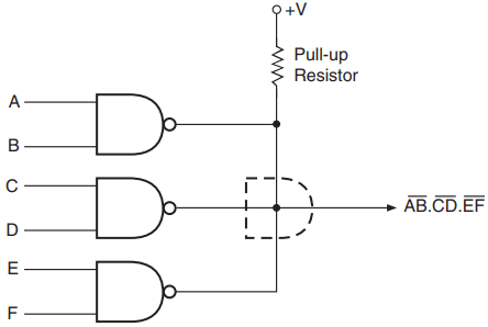
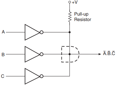
The advantage of using open collector/open drain gates lies in their capability of providing an ANDing operation when outputs of several gates are tied together through a common pull-up resistor, without having to use an AND gate for the purpose. This connection is also referred to as WIRE-AND connection.
Figure 15(a) shows such a connection for open collector NAND gates. The output in this case would be

Figure 15(b) shows a similar arrangement for NOT gates.
The disadvantage is that they are relatively slower and noisier. Open collector/drain devices are therefore not recommended for applications where speed is an important consideration.
Tristate Logic Gates
Tristate logic gates have three possible output states, i.e. the logic ‘1’ state, the logic ‘0’ state and a high-impedance state. The high-impedance state is controlled by an external ENABLE input. The ENABLE input decides whether the gate is active or in the high-impedance state. When active, it can be ‘0’ or ‘1’ depending upon input conditions.
One of the main advantages of these gates is that their inputs and outputs can be connected in parallel to a common bus line.
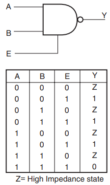
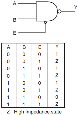
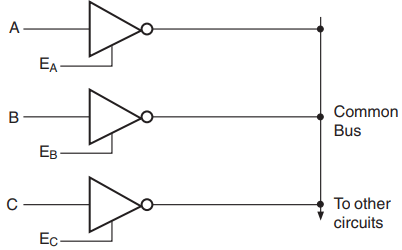
Figure 16(a) shows the circuit symbol of a tristate NAND gate with active HIGH ENABLE input, along with its truth table. The one shown in Fig. 16(b) has active LOW ENABLE input. When tristate devices are paralleled, only one of them is enabled at a time. Figure 17 shows paralleling of tristate inverters having active HIGH ENABLE inputs.
AND-OR-INVERT Logic Gates
AND-OR and OR-AND gates can be usefully employed to implement sum-of-products and product-of-sums Boolean expressions respectively. Figures 18(a) and (b) respectively show the symbols of AND-OR-INVERT and OR-AND-INVERT gates.
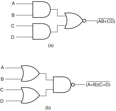
Another method for designating the gates shown in Fig. 18 is to call them two-wide, two-input AND-OR-INVERT or OR-AND-INVERT gates as the case may be. The gate is two-wide as there are two gates at the input, and two-input as each of the gates has two inputs.
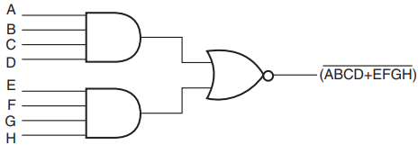
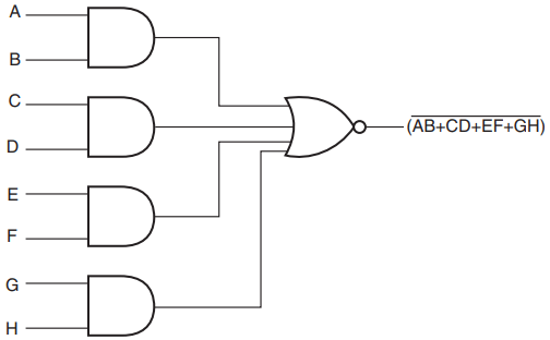
Other varieties such as two-wide, four-input AND-OR-INVERT (Fig. 19) and four-wide, two-input AND-OR-INVERT (Fig. 20) are also available in IC form.
Schmitt Logic Gates
The logic gates discussed so far have a single-input threshold voltage level. This threshold is the same for both LOW-to-HIGH and HIGH-to-LOW output transitions. This threshold voltage lies somewhere between the highest LOW voltage level and the lowest HIGH voltage level guaranteed by the manufacturer of the device. These logic gates can produce an erratic output when fed with a slow varying input.
Figure 21 shows the response of an inverter circuit when fed with a slow varying input both in the case of an ideal signal [Fig. 21(a)] and in the case of a practical signal having a small amount of AC noise superimposed on it [Fig. 21(b)].
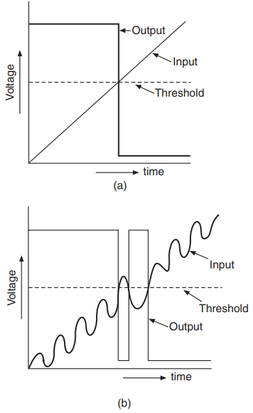
A possible solution to this problem lies in having two different threshold voltage levels, one for LOW-to-HIGH transition and the other for HIGH-to-LOW transition, by introducing some positive feedback in the internal gate circuitry, a phenomenon called hysteresis.
There are some logic gate varieties, mainly in NAND gates and inverters, that are available with built-in hysteresis. These are called Schmitt gates, which interpret varying input voltages according to two threshold voltages, one for LOW-to-HIGH and the other for HIGH-to-LOW output transition.
Figures 22(a) and (b) respectively show circuit symbols of Schmitt NAND and Schmitt inverter. Schmitt gates are distinguished from conventional gates by the small ‘hysteresis’ symbol reminiscent of the B − H loop for a ferromagnetic material. Figure 22(c) shows typical transfer characteristics for such a device.
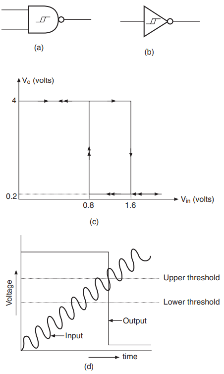
The difference between the two threshold levels is the hysteresis. These characteristics have been reproduced from the data sheet of IC 74LS132, which is a quad two-input Schmitt NAND belonging to the low-power Schottky TTL family.
Figure 22(d) shows the response of a Schmitt inverter to a slow varying noisy input signal. It may be mentioned here that hysteresis increases noise immunity and is used in applications where noise is expected on input signal lines.
Special Output Gates
There are many applications where it is desirable to have both non-inverted and inverted outputs. Examples include a single-input gate that is both an inverter and a non-inverting buffer, or a two-input logic gate that is both an AND and a NAND.
Such gates are called complementary output gates and are particularly useful in circuits where PCB space is at a premium. These are also useful in circuits where the addition of an inverter to obtain the inverted output introduces an undesirable time delay between inverted and non-inverted outputs.
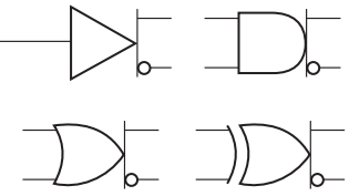
Figure 23 shows the circuit symbols of complementary buffer, AND, OR and EX-OR gates.
Related Posts
- Logic Gates
- Significance & Types of Logic Family
- Characteristics Parameters of Logic Families
- TTL Logic Family
- ECL Logic Family
- CMOS Logic Family
- Interfacing of Logic Families
- Microcontroller Architecture
- Components of Microcontroller
- Interfacing Devices with Microcontroller
- IC Based Multivibrator Circuits
- Astable, Monostable & Bistable Multivibrator
- Logic Analyser
- Types of Oscilloscope
- Frequency Synthesizers
- Frequency Counter