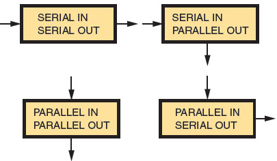
A shift register is a sequential logic circuit widely used to store data temporarily. Data can be loaded into and removed from a shift register in either a parallel or serial format. Figure 1 shows the four different methods of loading and reading data in a shift register.
Because of its ability to move data one bit at a time from one storage medium to another, the shift register is valuable in performing a variety of logic operations. Shift registers are constructed of flip-flops wired together. Flip-flops have all the functions necessary for a register: They can be reset, preset, toggled, or steered to a 1 or 0 level.
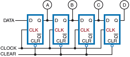
Figure 2 shows a basic shift register constructed from four flip-flops. It is called a 4-bit shift register because it consists of four binary storage elements.
A significant feature of the shift register is that it can move data to the right or left a number of bit positions. This is equivalent to multiplying or dividing a number by a specific factor. The data are shifted one bit position at a time for each input clock pulse. The clock pulses have full control over the shift register operations.
Operation of Shift Register
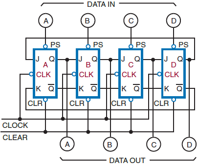
Figure 3 shows a typical 4-bit shift register constructed of JK flip-flops. The serial data and their complements are applied to the JK inputs of the A flip-flop. The other flip-flops are cascaded, with the outputs of one connected to the inputs of the next.
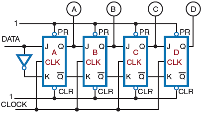
The toggles of all the flip-flops are connected together, and the clock pulse is applied to this line. Because all the flip-flops are toggled together, this is a synchronous circuit. Also, the clear inputs of each flip-flop are tied together to form a reset line. Data applied to the input are shifted through the flip-flops one bit position for each clock pulse.
For example, if the binary number 1011 is applied to the input of the shift register and a shift pulse is applied, the number stored in the shift register is shifted out and lost while the external number is shifted in.
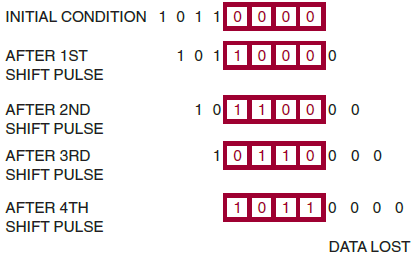
Figure 4 shows the sequence of events for storing a number in the shift register. One of the most common applications of a shift register is serial-to-parallel or parallel-to-serial data conversion. Figure 5 shows how a shift register can be loaded by a parallel input.
For parallel operations, the input data are preset into the shift register. Once the data are in the shift register, they can be shifted out serially, as discussed earlier. For serial-to-parallel data conversion, the data are initially shifted into the shift register with clock pulses.
Once the data are in the shift register, the outputs of the individual flip-flops are monitored simultaneously, and the data are routed to their destination. Shift registers can perform arithmetic operations such as multiplication or division.
Shifting a binary number stored in the shift register to the right has the same effect as dividing the number by some power of 2. Shifting the binary number stored in the shift register to the left has the same effect as multiplying the number by some power of 2.
Shift registers are a simple and inexpensive means of performing multiplication and division of numbers. Shift registers are often used for temporary storage. They are capable of storing one or more binary words.
There are three requirements for this application of a shift register: First, it must be able to accept and store data. Second, it must be able to retrieve or read out the data on command. Third, when the data are read, they must not be lost.
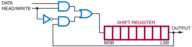
Figure 6 shows the external circuitry required to enable a shift register to read and maintain the data stored in it. The read/write line, when high, allows new data to be stored in the shift register. Once the data is stored, the read/write line goes low, enabling gate 2, which allows the data to recirculate while reading out the data.