Figure 1(a) shows a boost converter, another basic topology for converters. A boost converter always steps the voltage up. The theory of operation is similar to that for a buck converter in some ways but very different in others.
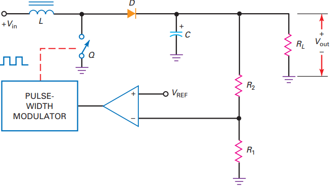
Boost Converter Working
For instance, when the pulse is high, the switch is closed and energy is stored in the magnetic field. When the pulse goes low, the switch opens. Again, the magnetic field around the inductor collapses and induces a reverse voltage across the inductor, as shown in Fig. 22-27b.
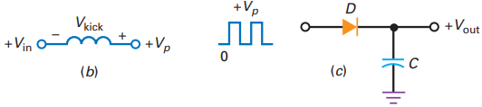
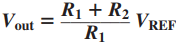
(c) capacitor-input filter produces output voltage equal to peak input.
Notice that the input voltage now adds to the inductive kick. This means that the peak voltage on the right end of the inductor is:
Vp = Vin + Vkick
The inductive kick depends on how much energy is stored in the magnetic field. Stated another way, Vkick is proportional to the duty cycle. With a stiff input voltage, a rectangular voltage waveform appears at the input to the capacitor-input filter of Fig. 1(c). Therefore, the regulated output voltage approximately equals the peak voltage given by the above Equation.
Because Vkick is always greater than zero, Vp is always greater than Vin. This is why a boost regulator always steps the voltage up. Aside from using a capacitor-input filter rather than a choke-input filter, the regulation with boost topology is similar to that with buck topology.
Because of the high gain of the comparator, the feedback almost equals the reference voltage. Therefore, the regulated output voltage is still given by the following Equation
If the output voltage tries to increase, there is more feedback voltage, resulting in less comparator output, a smaller duty cycle, and less inductive kick. This reduces the peak voltage, which offsets the attempted increase in output voltage.
If the output voltage tries to decrease, the smaller feedback voltage results in a larger peak voltage, which offsets the attempted decrease in output voltage.
Buck Boost Converter Working
Figure 2(a) shows a buck-boost converter, the third most basic topology for switching regulators. A buck-boost converter always produces a negative output voltage when driven by a positive input voltage.
When the PWM output is high, the switch is closed and energy is stored in the magnetic field. At this time, the voltage across the inductor equals Vin, with the polarity shown in Fig. 2(b).
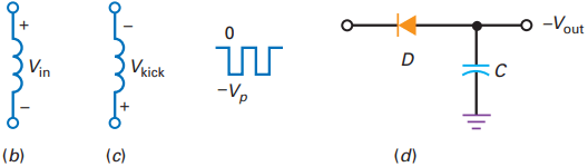
When the pulse goes low, the switch opens. Again, the magnetic field around the inductor collapses and induces a kick voltage across the inductor, as shown in Fig. 2(c). The kick voltage is proportional to the energy stored in the magnetic field, which is controlled by the duty cycle.
If the duty cycle is low, the kick voltage approaches zero. If the duty cycle is high, the kick voltage can be greater than Vin, depending on how much energy is stored in the magnetic field.
In Fig. 2(d), the magnitude of the peak voltage may be less than or greater than the input voltage. The diode and the capacitor-input filter then produce an output voltage equal to 2Vp. Since the magnitude of this output voltage can be less than or greater than the input voltage, the topology is called buck-boost.
An inverting amplifier is used in Fig. 2(a) to invert the feedback voltage before it reaches the inverting input of the comparator. The voltage regulation then works as previously described.
Attempted increases in output voltage reduce the duty cycle, which reduces the peak voltage. Attempted decreases in output voltage increase the duty cycle. Either way, the negative feedback holds the output voltage almost constant.
MAX631 Boost Converter Working
The MAX631 is a monolithic CMOS switching regulator that uses boost topology to produce a regulated output.
This low-power IC switching regulator has a switching frequency of 50 kHz, an input voltage of 2 to 5 V, and an efficiency of about 80 percent. The MAX631 is the ultimate in simplicity because it requires only two external components.
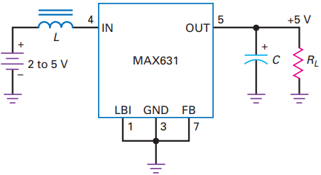
For instance, Fig. 3 shows a MAX631 connected as a boost regulator, producing a fixed output voltage of +5 V with an input voltage of +2 to +5 V. The input voltage often comes from a battery because one of the applications for these IC regulators is in portable instruments.
The data sheet recommends an inductor of 330 µH and a capacitor of 100 µF. The MAX631 is an 8-pin device whose unused pins are either grounded or left unconnected. In Fig. 3, pin 1 (LBI) can be used for low-battery detection. When grounded, it has no effect.
Although typically used as a fixed output regulator, the MAX631 can use an external voltage divider to provide a feedback voltage to pin 7 (FB). When pin 7 is grounded as shown, the output voltage is the factory preset value of +5 V.
Besides the MAX631, there is the MAX632, which produces an output of +12 V, and the MAX633, which produces an output of +15 V.
The MAX631 through MAX633 regulators include pin 6, called the charge pump, which is a low- impedance buffer that produces a rectangular output signal. This signal swings from 0 to Vout at the oscillator frequency and can be negatively clamped and peak-detected to get a negative output voltage.
For instance, Fig. 4(a) shows how a MAX633 uses its charge pump to get an output of approximately -12 V. C1 and D1 are a negative clamper. D2 and C2 are a negative peak detector. Here is how the charge pump works:
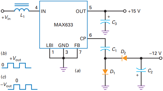
(c) input to negative peak detector
Figure 4(b) shows the ideal voltage waveform coming out of pin 6. Because of the negative clamper, the ideal voltage waveform across D1 is the negatively clamped waveform of Fig. 4(c).
This waveform drives the negative peak detector to produce an output of approximately -12 V at 20 mA. The magnitude of this voltage is approximately 3 V less than the output voltage because of the two diode drops (D1 and D2) and the drop across the output impedance of the buffer (around 30 V).
If we use a battery to supply the input voltage to a linear regulator, the output voltage is always smaller. Boost regulators not only have better efficiency than linear regulators, they also can step up the voltage in a battery-powered system.
This is very important and explains why monolithic boost regulators are so widely used. The availability of low-cost rechargeable batteries has made the monolithic boost regulator a standard choice for battery-powered systems.
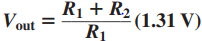
The MAX631 through MAX633 devices have an internal reference voltage of 1.31 V. When these switching regulators are used with an external voltage divider, the following equation gives the regulated output voltage:
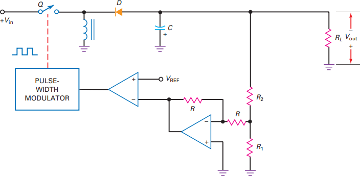
LT1074 Buck Boost Converter Working
The internal design of the LT1074 can support a buck-boost external connection. Figure 5 shows the LT1074 connected as a buck-boost converter. Again, we are using a Schottky diode to improve the efficiency.
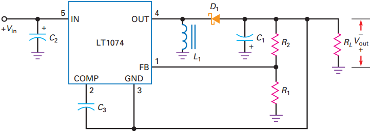
As previously discussed, energy is stored in the inductor’s magnetic field when the internal switch is closed. When the switch opens, the magnetic field collapses and forward-biases the diode. The negative kick voltage across the inductor is peak-detected by the capacitor-input filter to produce -Vout.
In the earlier discussion of buck-boost topology, we used an inverting amplifier to get a positive feedback voltage because the output sample from the voltage divider was negative. The internal design of the LT1074 takes care of this problem.
The data sheet recommends returning the GND pin to the negative output voltage, as shown in Fig. 5. This produces the correct error voltage to the comparator that controls the pulse-width modulator.
Related Posts
- P N Junction Diode Theory | Working
- Characteristics of PN Junction Diode
- Working Principle of Rectifier
- Zener Diode Characteristics
- Zener Diode as Voltage Regulator
- JFET | Junction Field Effect Transistor Basics
- JFET Construction and Working
- Op Amp | Operational Amplifier Basics
- Transistor as a Switch
- Buck Converter Working
- Buck Boost Converter Working
- Astable & Monostable Operation of 555 Timer Chip
- Light Sensitive Devices
- Industrial Applications of Ultrasonic Waves
- Radar Working Principle
- Electrical Timer & Timer Charts
- RLC Parallel & RLC Series Circuit Resonance
- Types of Capacitors