Figure 1(a) shows a buck converter, the most basic topology for converters. A buck converter always steps the voltage down. A transistor, either a bipolar junction or a power FET, is used as the switching device.

A rectangular signal out of the pulse-width modulator closes and opens the switch. A comparator controls the duty cycle of the pulses.
For instance, the pulse-width modulator may be a one-shot multivibrator with a comparator driving the control input. With a monostable 555 timer, an increase in control voltage increases the duty cycle.
Buck Converter Working
When the pulse is high, the switch is closed. This reverse-biases the diode so that all the input current flows through the inductor. This current creates a magnetic field around the inductor. The amount of stored energy in the magnetic field is given by:
Energy = 0.5Li2
The current through the inductor also charges the capacitor and supplies current to the load. While the switch is closed, the voltage across the inductor has the plus-minus polarity shown in Fig. 1(b).

dc value to output.
As the current through the inductor increases, more energy is stored in the magnetic field.
When the pulse goes low, the switch opens. At this instant, the magnetic field around the inductor starts collapsing and induces a reverse voltage across the inductor, as shown in Fig. (c). This reverse voltage is called the inductive kick.
Because of the inductive kick, the diode is forward biased and the current through the inductor continues to flow in the same direction.
At this time, the inductor is returning its stored energy to the circuit. In other words, the inductor acts like a source and continues supplying current for the load.
Current flows through the inductor until the inductor returns all its energy to the circuit (discontinuous mode) or until the switch closes again (continuous mode), whichever comes first. In either case, the capacitor will also source load current during part of the time that the switch is open. This way, the ripple across the load is minimized.
The switch is being continuously closed and opened. The frequency of this switching can be from 10 to more than 100 kHz. (Some IC regulators switch at more than 1 MHz.)
The current through the inductor is always in the same direction, passing through either the switch or the diode at different times in the cycle. With a stiff input voltage and an ideal diode, a rectangular voltage waveform appears at the input to the choke-input filter (see Fig. 1(d).
The output of a choke-input filter equals the dc or average value of the input to the filter. The average value is related to the duty cycle and is given by:
Vout = DVin
The larger the duty cycle, the larger the dc output voltage.
When the power is first turned on, there is no output voltage and no feedback voltage from the R1-R2 voltage divider. Therefore, the comparator output is very large and the duty cycle approaches 100 percent.
As the output voltage builds up, however, the feedback voltage VFB reduces the comparator output, which reduces the duty cycle. At some point, the output voltage reaches an equilibrium value at which the feedback voltage produces a duty cycle that gives the same output voltage.
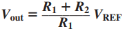
Because of the high gain of the comparator, the virtual short between the input terminals of the comparator means that:
VFB ≈ VREF
From this, we can derive this expression for the output voltage:
After equilibrium sets in, any attempted change in the output voltage, whether caused by line or load changes, will be almost entirely offset by the negative feedback.
For instance, if the output voltage tries to increase, the feedback voltage reduces the comparator output. This reduces the duty cycle and the output voltage. The net effect is only a slight increase in output voltage, much less than without the negative feedback.
Similarly, if the output voltage tries to decrease because of a line or load change, the feedback voltage is smaller and the comparator output is larger. This increases the duty cycle and produces a larger output voltage that offsets almost all the attempted decrease in output voltage.
LT1074 Buck Converter Working
Some IC switching regulators have only five external pins. For instance, the LT1074 is a monolithic bipolar switching regulator that uses buck topology. It contains most of the components discussed earlier, such as a reference voltage of 2.21 V, a switching device, an internal oscillator, a pulse-width modulator, and a comparator.
It runs at a switching frequency of 100 kHz, can handle input voltages from 18 to 140 V dc, and has an efficiency of 75 to 90 percent for load currents from 1 to 5 A.

Figure 2 shows an LT1074 connected as a buck regulator.
- Pin 1 (FB) is for the feedback voltage.
- Pin 2 (COMP) is for frequency compensation to prevent oscillations at higher frequencies.
- Pin 3 (GND) is ground.
- Pin 4 (OUT) is the switched output of the internal switching device.
- Pin 5 (IN) is for the dc input voltage.
D1, L1, C1, R1, and R2 serve the same functions as described in the earlier discussion of a buck regulator.
But notice the use of a Schottky diode to improve the efficiency of the regulator. Because the Schottky diode has a lower knee voltage, it wastes less power.
The data sheet of an LT1074 recommends adding a capacitor C2 from 200 to 470 µF across the input for line filtering. Also recommended are a resistor R3 of 2.7 kΩ and a capacitor C3 of 0.01 µF to stabilize the feedback loop (prevent oscillations).
The LT1074 is widely used. A look at Fig. 2 tells us why. The circuit is incredibly simple, considering that it is a switching regulator, one of the most difficult of all circuits to design and build in discrete form.
Fortunately, the IC designers have done all the hard work because the LT1074 includes everything except the components that cannot be integrated (choke and filter capacitors) and those left for the user to select (R1 and R2).
By selecting values for R1 and R2, we can get regulated output voltage from about 2.5 to 38 V. Since the reference voltage of an LT1074 is 2.21 V, the output voltage is given by:

The headroom voltage should be at least 2 V because the internal switching device consists of a pnp transistor driving an npn Darlington. The overall switch drop can be as high as 2V with high currents.
Related Posts
- P N Junction Diode Theory | Working
- Characteristics of PN Junction Diode
- Working Principle of Rectifier
- Zener Diode Characteristics
- Zener Diode as Voltage Regulator
- JFET | Junction Field Effect Transistor Basics
- JFET Construction and Working
- Op Amp | Operational Amplifier Basics
- Transistor as a Switch
- Buck Converter Working
- Buck Boost Converter Working
- Astable & Monostable Operation of 555 Timer Chip
- Light Sensitive Devices
- Industrial Applications of Ultrasonic Waves
- Radar Working Principle
- Electrical Timer & Timer Charts
- RLC Parallel & RLC Series Circuit Resonance
- Types of Capacitors