There are two types of extrinsic semiconductors. These are n-type and p-type. In n-type, the electrons are majority charge carriers while holes are minority charge carriers. In p-type, the holes are majority charge carriers and electrons are minority charge carriers.
When these two types of materials namely n-type and p-type are chemically combined with a special fabrication technique to form a p-n junction an electronic device called diode is formed. On p side, there are a large number of holes while on n side there are a large number of free electrons.
Hence overall p-n junction acts as non-uniformly doped material. Hence the overall there is a non-uniform distribution of charge carriers. When such a non-uniform distribution exists then the charge carriers start moving from high concentration area towards the low concentration area. This is termed as diffusion.
P-N Junction Diode Theory
In an unbiased p-n junction, the majority holes on the p side start diffusing into the n side while the majority free electrons on the n side start diffusing into the p side.
In the n region, the holes diffusing from the n-side, recombine with free electrons. Thus due to additional positively charged holes, these atoms on the n-side become positive immobile ions, just near the junction in n region.
In the p region, the free electrons diffusing from the n-side, recombine with the holes of the atoms. Thus due to the gain of additional negatively charged free electrons, these atoms become negative immobile ions, just near the junction in p-region.
As more holes diffuse on the n side, a large immobile positive charge accumulates near the junction on n side. This positive charge repels the positively charged holes and the further diffusion of holes stops.
Similarly large negative charge accumulates near the junction on the p side. This negative charge repels the negatively charged electrons and the further diffusion of electrons stops.
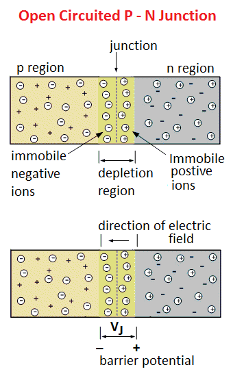
Thus there exists a wall near the junction with a negative immobile charge on the p side and positive immobile charge on the n side. There are no charge carriers in this region. The region is depleted off the charge carriers hence called depletion region or depletion layer.
In equilibrium condition, the depletion region gets widened up to a point where no further electrons or holes can cross the junction. Thus it acts as a barrier.
Barrier Potential of Junction Diode
Due to immobile positive ions on the n side and immobile negative ions on the p side, there exists an electric field across the junction. This creates a potential difference across the depletion region which acts as a barrier. This is termed as barrier potential or junction potential of the p-n junction diode. It is denoted by VJ or Vo. For the silicon diodes, it is 0.6 V and for the germanium diodes, it is 0.2 V. The barrier potential depends on:
- Type of semiconductor
- Donor impurity added
- Acceptor impurity added
- Temperature
Effect of Temperature on Barrier Potential
The physical distance from one side to the other side of the depletion region is called the width of the depletion region. Practically, the width of the depletion region is about 0.5 to 1 micron. (1 micron = 10-6 m).
As temperature increases, the width of the depletion region decreases and the barrier potential decreases. The barrier potential decreases by approximately 2.5 mV per degree Celsius rise in temperature.
P-N Junction Diode Working
The p-n junction forms a popular semiconductor device called p-n junction diode. The p-n junction diode has two terminals called electrodes, one each from p-region and n-region.
To connect the n and p-regions to the external terminals, a metal is applied to the heavily doped n and p-type semiconductor regions. Such a contact between a metal and a heavily doped semiconductor is called ohmic contact.
This ohmic contact conducts current equally in both the directions and the voltage drop across the contact is very small, which does not affect the performance of the device.
The p-region acts as the anode while the n-region acts as the cathode. The arrowhead in the symbol indicates the direction of the conventional current, which can flow when an external voltage is connected in a specific manner across the diode. The p-n junction diode allows current flow only in one direction, under biased condition.
Applying external d.c. voltage to any electronic device is called biasing. Depending upon the polarity of the d.c. voltage externally applied to it, the biasing is classified as forward biasing and reverse biasing.
Forward Biasing of Diode
When an external d.c. voltage is connected in such a way that the p-region is connected to positive and the n region to negative of the d.c. voltage then the biasing is called forward biasing.
In this state, the negative of battery pushes the free electrons against the barrier from n to p-region while positive of battery pushes holes against barrier from p to n-region. Due to this, the width of the depletion region reduces and consequently, the barrier potential also reduces.
As the applied voltage is increased, at a particular value, the depletion region becomes very narrow and majority charge carriers can easily cross the junction. This large number of majority charge carriers constitute a current called forward current.
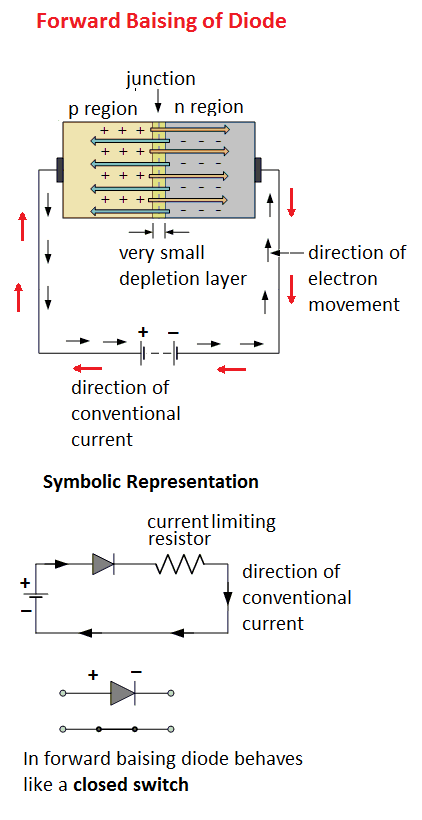
So the current can easily pass through the diode and we can say the diode behaves like a closed switch in the forward biasing state.
The current in the p-region is due to the movement of holes so it is a hole current. The current in the n region is due to the movement of electrons so it is an electron current. The holes in p-region and electrons in n-region are majority charge carriers. Hence the forward current is due to majority charge carriers.
Reverse Biasing of Diode
When an external d.c. voltage is connected in such a way that p-region is connected to negative and n region to the positive terminal of the d.c. voltage then the biasing is called reverse biasing.
In the reverse biasing of a diode, the negative of battery attracts the holes in p-region and positive of battery attracts the electrons in n region away from the junction. This widens the depletion region and increases the barrier potential. No majority charge carrier can cross the junction.
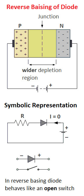
Hence the resistance of the reversed biased diode is very high and the diode remains non-operative in this state. The diode behaves like an open switch in the reverse biasing state.
However, due to increased barrier potential, the free electrons on the p side are dragged towards positive while holes on the n side are dragged towards the negative of the battery. This constitutes a current called reverse current. It flows due to minority charge carriers and hence its magnitude is very very small.
For constant temperature, the reverse current is almost constant though applied reverse voltage is increased up to a certain limit. Hence it is called reverse saturation current denoted by Io. It is in the order of a few micro-amperes for Ge and a few nano-amperes for Si diodes.
Breakdown Mechanisms in Junction Diode
If the reverse voltage is increased beyond particular value, a large reverse current can flow damaging the diode. This is called the reverse breakdown of the diode. Such a reverse breakdown of a diode can take place due to the following two effects,
- Avalanche effect and,
- Zener effect
Breakdown of Diode due to Avalanche Effect
If the reverse voltage is increased, at a particular value, the velocity of minority carriers increases. Due to the kinetic energy associated with the minority carriers, more minority carriers are generated when there is a collision of minority carriers with the atoms. The collision makes the electrons to break the covalent bonds.
These electrons are available as minority carriers and get accelerated due to high reverse voltage. They again collide with other atoms to generate more minority carriers. This is called the carrier multiplication.
Finally, a large number of minority carriers move across the junction, breaking the p-n junction. These large number of minority carriers give rise to a very high reverse current.
This effect is called the Avalanche effect and the mechanism of destroying the junction is called the reverse breakdown of a p-n junction. The voltage at which the breakdown of a p-n junction occurs is called the reverse breakdown voltage.
Breakdown of Diode due to Zener Effect
When a p-n junction is heavily doped the depletion region is very narrow. Due to the narrow depletion region on high reverse voltage, the electric field becomes very intense across the depletion region. Such an intense field is enough to pull the electrons out of the valence bands of the stable atoms.
Such a creation of free electrons is called the zener effect which is different from the avalanche effect. These minority carriers constitute a very large current and the mechanism is called zener breakdown of the diode.
These effects are required to be considered for special diodes such as zener diodes as such diodes are always operated in reverse breakdown condition.
Related Posts
- P N Junction Diode Theory | Working
- Characteristics of PN Junction Diode
- Working Principle of Rectifier
- Zener Diode Characteristics
- Zener Diode as Voltage Regulator
- JFET | Junction Field Effect Transistor Basics
- JFET Construction and Working
- Op Amp | Operational Amplifier Basics
- Transistor as a Switch
- Buck Converter Working
- Buck Boost Converter Working
- Astable & Monostable Operation of 555 Timer Chip
- Light Sensitive Devices
- Industrial Applications of Ultrasonic Waves
- Radar Working Principle
- Electrical Timer & Timer Charts
- RLC Parallel & RLC Series Circuit Resonance
- Types of Capacitors