The bipolar junction transistor is a current-controlled device, while the field-effect transistor (FET) is a voltage-controlled device. The field-effect transistor uses basically no input current. Instead, output current flow is controlled by a varying electric field, which is created through the application of a voltage. This is the origin of the term field effect.
The field-effect transistor was designed to get around the two major disadvantages of the bipolar junction transistor: low switching speed and high drive power, which are imposed by the base current.
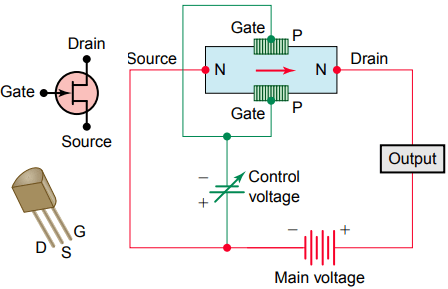
The junction field-effect transistor (JFET) is shown in Figure 1. It is constructed with a bar of N-type material and a gate of P-type material. Because the material in the channel is N type, the device is called an N-channel JFET.
JFET | Junction Field Effect Transistor Basics
JFETs have three connections, or leads: source, gate, and drain. These correspond to the emitter, base, and collector of the bipolar transistor, respectively. The names of the terminals refer to their functions.
The gate terminal may be thought of as controlling the opening and closing of a physical gate. This gate permits electrons to flow through or blocks their passage by creating or eliminating a channel between the source and drain.
Field-effect transistors are unipolar; their working current flows through only one type of semiconductor material. This is in contrast to bipolar transistors, which have current flowing through both N-type and P-type regions.
There are also P-channel JFETs that use P-type material for the channel and N-type material for the gate. The main difference between the N- and P-types is that the polarities of voltage they are connected to are opposite.
The JFET operates in the depletion mode, which means it is normally on. If a source of voltage is connected to the source and drain, and no source of voltage is connected to the gate, current is free to flow through the channel.

Figure 2 illustrates the gate voltage control of current through an N-channel JFET. The operation of the circuit can be summarized as follows:
• The normal polarities for biasing the N-channel JFET are as indicated. Note that the JFET is normally operated with the control voltage connected to the source and gate junction in reverse bias. The result is very high input impedance.
• If a source voltage is connected to the source and drain, and no control voltage is connected to the gate, electrons are free to flow through the channel.
• A negative voltage connected to the gate increases the channel resistance and reduces the amount of current flow between the source and the drain.
• Thus, the gate voltage controls the amount of drain current, and the control of this current is almost powerless.
• Continuing to increase the negative gate voltage to the pinch-off point will reduce the drain current to a very low value, effectively zero.
Metal Oxide Semiconductor Field Effect Transistor (MOSFET)
The metal oxide semiconductor field-effect transistor (MOSFET) is by far the most common field-effect transistor. Field-effect transistors do not require any gate current for operation so the gate structure can be completely insulated from the channel.
The gate of a JFET consists of a reverse-biased junction, whereas the gate of a MOSFET consists of a metal electrode insulated by metal oxide from the channel. The insulated gate of a MOSFET has much higher input impedance than the JFET, so it is even less of a load on preceding circuits.
Because the oxide layer is extremely thin, the MOSFET is susceptible to destruction by electrostatic charges. Special precautions are necessary when handling or transporting MOS devices.
The MOSFET can be made with a P channel or an N channel. The action of each is the same, but the polarities are reversed. In addition, there are two types of MOSFETs: depletion-mode MOSFETs, or D type, and enhancement-mode MOSFETs, or E type. Symbols used for N- and P-channel depletion-mode MOSFETs are shown in Figure 3.

The channel is represented as a solid line to signify that the circuit between the drain and source is normally complete and that the device is normally on. Gate voltage in a MOSFET circuit can be of either polarity, since a diode junction is not used. This makes the enhancement mode of operation possible.
The enhancement-mode MOSFET is normally off, which means that if a voltage is connected to the drain and source and no voltage is connected to the gate, there will be no current flow through the device.
The proper gate voltage will attract carriers to the gate region and form a conductive channel. Thus the channel is considered to be “enhanced,” or aided by gate voltage.

Figure 4 shows the schematic symbols used for enhancement-mode MOSFETs. Note that, unlike the depletion mode symbols, the line from the source to drain is broken. This implies that the device is normally off.
Figure 5 shows an enhancement-mode MOSFET used as part of an off-delay cube timer circuit. Because the gate current flow is negligible, a broad range of time-delay periods, from minutes to hours, is possible. The operation of the circuit can be summarized as follows:

• With the switch initially open, a voltage is applied between the drain and source but no voltage is applied between the gate and source. Therefore, no current flows through the MOSFET and the relay coil will be de-energized.
• Closing the switch results in a positive voltage being applied to the gate, which triggers the MOSFET into conduction to energize the relay coil and switch the state of its contacts.
• At the same time the capacitor is charged to 12 V DC.
• The circuit remains in this state with the relay coil energized as long as the switch remains closed.
• When the switch is opened, the timing action begins.
• The positive gate circuit to the 12-V source is opened.
• The stored positive charge of the capacitor keeps the MOSFET switched on.
• The capacitor begins to discharge its stored energy through R1 and R2 while still maintaining a positive voltage at the gate.
• The MOSFET and relay coil continue to conduct a current for as long as it takes the capacitor to discharge.
• The discharge rate, and thus the off-delay timing period, is adjusted by varying the resistance of R2. Increasing the resistance will slow the rate of discharge and increase the timing period. Decreasing the resistance will have the opposite effect.
Power MOSFETs
Power MOSFETs that are designed to handle larger amounts of current are used in some electronic DC motor speed controllers. For this type of application, the MOSFET is used to switch the applied DC voltage on and off very rapidly.
The speed of a DC motor is directly proportional to the voltage applied to the armature. By switching the DC motor line voltage, it is possible to control the average voltage applied to the motor armature.

Figure 6 shows an enhancement-mode power MOSFET used as part of a chopper circuit. In this circuit the source voltage is chopped by the MOSFET to produce an average voltage somewhere between 0 and 100 percent of the DC supply voltage. The operation of the circuit can be summarized as follows:
• The DC supply and motor field voltage is fixed and the voltage applied to the motor armature is varied by the MOSFET using a technique called pulse-width modulation (PWM).
• Pulse-width modulation works by applying a series of modulated square wave pulses to the gate.
• Motor speed is controlled by driving the motor with short pulses. These pulses vary in duration to change the speed of the motor. The longer the pulses, the faster the motor runs and vice versa.
• By adjusting the duty cycle of the gate signal (modulating the width of the pulse), the time fraction that the MOSFET is on can be varied, along with the average voltage to the motor armature and hence the motor speed.
• The diode (sometimes called a freewheeling diode) is connected in reverse bias to provide a discharge path for the collapsing magnetic field when voltage to the motor armature is switched off.
Insulated Gate Bipolar Transistor (IGBT)
The insulated-gate bipolar transistor (IGBT) is a cross between a bipolar transistor and MOSFET in that it combines the positive attributes of both.
BJTs have lower on resistance, but have longer switching times, especially at turn-off. MOSFETs can be turned on and off much faster, but their on-state resistance is higher.
IGBTs have lower on-state power loss in addition to faster switching speeds, allowing the electronic motor drive to operate at much higher switching frequencies and control more power.

The two different schematic symbols used to represent an N-type IGBT and its equivalent circuit are shown in Figure 7. Notice that the IGBT has a gate like a MOSFET yet it has an emitter and a collector like a BJT.
The equivalent circuit is depicted by a PNP transistor, where the base current is controlled by a MOS transistor. In essence, the IGFET controls the base current of a BJT, which handles the main load current between collector and emitter.
This way, there is extremely high current gain (since the insulated gate of the IGFET draws practically no current from the control circuitry), but the collector-to-emitter voltage drop during full conduction is as low as that of an ordinary BJT.
As applications for IGBT components have continued to expand rapidly, semiconductor manufacturers have responded by providing IGBTs in both discrete (individual) and modular packages.

Figure 8 shows a power electronic module that houses two insulated-gate bipolar power transistors and corresponding diodes. This package provides an easy way to cool the devices and to connect them to the outer circuit. Figure 9 illustrates how IGBTs are used in an electronic variable-frequency AC motor drive.
A variable-frequency drive controls the speed of the AC motor by varying the frequency supplied to the motor. In addition, the drive also regulates the output voltage in proportion to the output frequency to provide a relatively constant ratio of voltage to frequency (V/Hz), as required by the characteristics of the AC motor to produce adequate torque.

The six IGBTs are capable of very high switching speeds and may be required to switch the voltage to the motor thousands of times per second. The operation of the circuit can be summarized as follows:
• The input section of the drive is the converter. It contains six diodes, arranged in an electrical bridge. The diodes convert the three-phase AC power to DC power.
• The next section—the DC bus—sees a fixed DC voltage.
• The inductor (L) and the capacitor (C) work together to filter out any AC component of the DC waveform. The smoother the DC waveform, the cleaner the output waveform from the drive.
• The DC bus feeds the inverter, the final section of the drive. As the name implies, this section inverts DC voltage back to AC. But it does so in a variable voltage and frequency output.
• Fairly involved control circuitry coordinates the switching of the IGBT devices, typically through a logic control board that dictates the firing of power components in proper sequence.
Related Posts
- P N Junction Diode Theory | Working
- Characteristics of PN Junction Diode
- Working Principle of Rectifier
- Zener Diode Characteristics
- Zener Diode as Voltage Regulator
- JFET | Junction Field Effect Transistor Basics
- JFET Construction and Working
- Op Amp | Operational Amplifier Basics
- Transistor as a Switch
- Buck Converter Working
- Buck Boost Converter Working
- Astable & Monostable Operation of 555 Timer Chip
- Light Sensitive Devices
- Industrial Applications of Ultrasonic Waves
- Radar Working Principle
- Electrical Timer & Timer Charts
- RLC Parallel & RLC Series Circuit Resonance
- Types of Capacitors